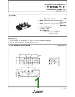
MITSUBISHI THYRISTOR MODULES
TM10T3B-M,-H
MEDIUM POWER GENERAL USE
INSULATED TYPE
ABSOLUTE MAXIMUM RATINGS
Voltage class
Symbol
Parameter
Unit
M
H
VRRM
Repetitive peak reverse voltage
Non-repetitive peak reverse voltage
DC reverse voltage
400
480
320
400
480
320
800
960
640
800
960
640
V
V
V
V
V
V
VRSM
VR (DC)
VDRM
VDSM
VD (DC)
Repetitive peak off-state voltage
Non-repetitive peak off-state voltage
DC off-state voltage
Symbol
Parameter
DC output current
Conditions
Ratings
20
Unit
A
IO
3-phase fullwave rectified, TC=79°C
One half cycle at 60Hz, peak value
Value for one cycle of surge current
ITSM, IFSM
Surge (non-repetitive) current
200
A
2
2
2
2
I t
I t for fusing
1.7 × 10
50
A s
di/dt
PGM
PG (AV)
VFGM
VRGM
IFGM
Tj
Critical rate of rise of on-state current VD=1/2VDRM, IG=0.5A, Tj=125°C
Peak gate power dissipation
A/µs
W
5.0
Average gate power dissipation
Peak gate forward voltage
0.5
W
10
V
Peak gate reverse voltage
5.0
V
Peak gate forward current
2.0
A
Junction temperature
–40~125
–40~125
2500
0.98~1.47
10~15
130
°C
Tstg
Storage temperature
°C
Viso
Isolation voltage
Mounting torque
Weight
Charged part to case
Mounting screw M4
Typical value
V
N·m
kg·cm
g
—
—
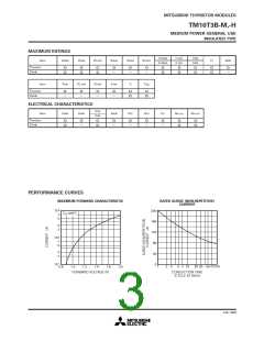
ELECTRICAL CHARACTERISTICS
Limits
Typ.
—
Symbol
Parameter
Test conditions
Unit
Min.
—
Max.
4.0
4.0
1.3
—
IRRM
Repetitive peak reverse current
Repetitive peak off-state current
Forward voltage
Tj=125°C, VRRM applied
Tj=125°C, VDRM applied
mA
mA
V
—
—
IDRM
—
—
VTM, VFM
dv/dt
VGT
Tj=125°C, ITM=IFM=20A, instantaneous meas.
500
—
—
Critical rate of rise of off-state voltage Tj=125°C, VD=2/3VDRM
V/µs
V
—
2.0
—
Gate trigger voltage
Tj=25°C, VD=6V, RL=2Ω
0.25
10
—
VGD
Gate non-trigger voltage
Gate trigger current
Tj=125°C, VD=1/2VDRM
V
—
50
IGT
Tj=25°C, VD=6V, RL=2Ω
mA
°C/W
°C/W
—
—
4.5
0.6
Rth (j-c)
Rth (c-f)
Thermal resistance
Junction to case (per 1/6 module)
Case to fin, Conductive grease applied (per 1/6 module)
—
—
Contact thermal resistance
Measured with a 500V megohmmeter between main terminal
and case
10
—
—
—
Insulation resistance
MΩ
Note: Items of the above table applies to the Thyristor part and the Diode part as circled in the following tables.
Feb.1999

 MITSUBISHI [ Mitsubishi Group ]