MITSUBISHI MICROCOMPUTERS
3822 Group
SINGLE-CHIP 8-BIT CMOS MICROCOMPUTER
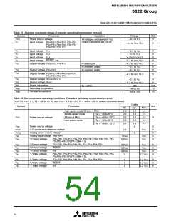
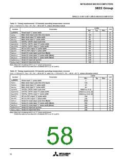
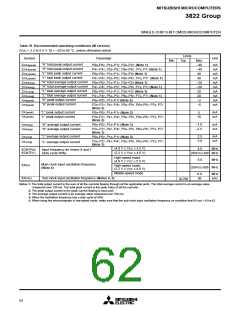
Table 31 Timing requirements 1 (Extended operating temperature version)
(VCC = 4.0 to 5.5 V, VSS = 0 V, Ta = –40 to 85 °C, unless otherwise noted)
Limits
Unit
Symbol
Parameter
Min.
2
Typ.
Max.
tw(RESET)
tc(XIN)
Reset input “L” pulse width
µs
ns
ns
ns
ns
ns
ns
ns
ns
ns
ns
ns
ns
ns
Main clock input cycle time (XIN input)
Main clock input “H” pulse width
125
45
twH(XIN)
twL(XIN)
Main clock input “L” pulse width
40
tc(CNTR)
twH(CNTR)
twL(CNTR)
twH(INT)
twL(INT)
tc(SCLK)
CNTR0, CNTR1 input cycle time
250
105
105
80
CNTR0, CNTR1 input “H” pulse width
CNTR0, CNTR1 input “L” pulse width
INT0 to INT3 input “H” pulse width
INT0 to INT3 input “L” pulse width
Serial I/O clock input cycle time (Note)
Serial I/O clock input “H” pulse width (Note)
Serial I/O clock input “L” pulse width (Note)
Serial I/O input set up time
80
800
370
370
220
100
twH(SCLK)
twL(SCLK)
t
su(RXD–SCLK)
th(SCLK–RXD) Serial I/O input hold time
Note: When bit 6 of address 001A16 is “1” (clock synchronous).
Divide this value by four when bit 6 of address 001A16 is “0” (UART).
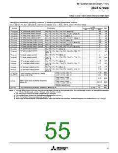
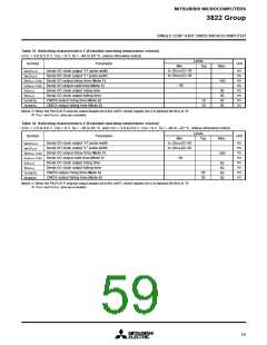
Table 32 Timing requirements 2 (Extended operating temperature version)
(VCC = 2.0 to 4.0 V, VSS = 0 V, Ta = –20 to 85 °C, and VCC = 3.0 to 4.0 V, Ta = –40 to –20 °C, unless otherwise noted)
Limits
Symbol
Parameter
Unit
Min.
Typ.
Max.
tw(RESET)
tc(XIN)
Reset input “L” pulse width
2
µs
ns
ns
ns
ns
ns
ns
ns
ns
ns
ns
ns
ns
ns
Main clock input cycle time (XIN input)
Main clock input “H” pulse width
125
twH(XIN)
twL(XIN)
45
Main clock input “L” pulse width
40
tc(CNTR)
twH(CNTR)
twL(CNTR)
twH(INT)
twL(INT)
tc(SCLK)
CNTR0, CNTR1 input cycle time
900/(VCC–0.4)
CNTR0, CNTR1 input “H” pulse width
CNTR0, CNTR1 input “L” pulse width
INT0 to INT3 input “H” pulse width
INT0 to INT3 input “L” pulse width
Serial I/O clock input cycle time (Note)
Serial I/O clock input “H” pulse width (Note)
Serial I/O clock input “L” pulse width (Note)
Serial I/O input set up time
450/(VCC–0.4)–20
450/(VCC–0.4)–20
230
230
2000
950
950
400
200
twH(SCLK)
twL(SCLK)
tsu(RXD–SCLK)
th(SCLK–RXD) Serial I/O input hold time
Note: When bit 6 of address 001A16 is “1” (clock synchronous).
Divide this value by four when bit 6 of address 001A16 is “0” (UART).
58

 MITSUBISHI [ Mitsubishi Group ]