MITSUBISHI MICROCOMPUTERS
7477/7478 GROUP
SINGLE-CHIP 8-BIT CMOS MICROCOMPUTER
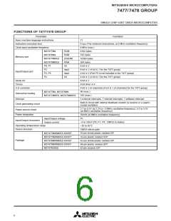
FUNCTIONAL DESCRIPTION
Central Processing Unit (CPU)
The 7477/7478 group uses the standard 740 family instruction set.
Refer to the table of 740 family addressing modes and machine in-
structions or the SERIES 740 <Software> User’s Manual for
details on the instruction set.
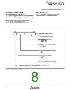
CPU Mode Register
The CPU mode register is allocated at address 00FB16.
This register contains the stack page selection bit.
Machine-resident 740 family instructions are as follows:
The FST and SLW instruction cannot be used.
The MUL, DIV, WIT, and STP instruction can be used.
b7
b0
CPU mode register (Address 00FB 16
)
These bits must always be set to “0”.
Stack page selection bit (Note 1)
0 : In page 0 area
1 : In page 1 area
P5
0 : P5
1 : XCIN, XCOUT
0
, P5
1/XCIN, XCOUT selection bit (Note 2)
0
, P5
1
X
COUT drive capacity selection bit (Note 2)
0 : Low
1 : High
Clock (XIN-XOUT) stop bit (Note 2)
0 : Oscillates
1 : Stops
Internal system clock selection bit (Note 2)
0 : XIN-XOUT selected (normal mode)
1 : XCIN-XCOUT selected (low-speed mode)
Notes 1 : In the M37477M4-XXXSP/FP, M37478M4-XXXSP/FP, set this bit to “0”.
2 : In the 7477 group, set this bit to “0”.
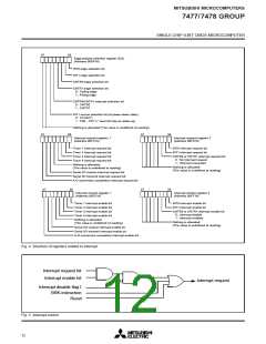
Fig. 1 Structure of CPU mode register
8

 MITSUBISHI [ Mitsubishi Group ]