MITSUBISHI MICROCOMPUTERS
7477/7478 GROUP
SINGLE-CHIP 8-BIT CMOS MICROCOMPUTER
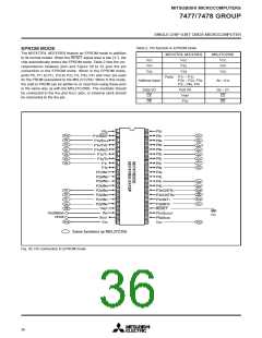
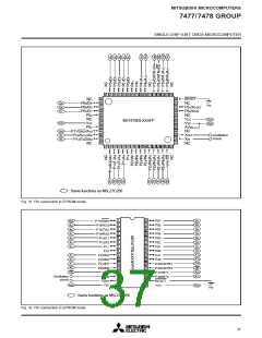
PROM READING AND WRITING
NOTES ON HANDLING
Reading
(1) Sunlight and fluorescent light contain wave lengths capable of
erasing data. For ceramic package types, cover the transpar-
ent window with a seal (provided) when this chip is in use.
However, this seal must not contact the lead pins.
To read the PROM, set the CE and OE pins to “L” level. Input the
address of the data (A0 to A14) to be read and the data will be out-
put to the I/O pins (D0 to D7). The data I/O pins will be floating
when either the CE or OE pin is in the “H” state.
(2) Before erasing, the glass should be cleaned and stains such
as finger prints should be removed thoroughly. If these stains
are not removed, complete erasure of the data could be pre-
vented.
Writing
To write to the PROM, set the OE pin to “H” level. The CPU will en-
ter the program mode when VPP is applied to the VPP pin. The
address to be written to is selected with pins A0 to A14, and the
data to be written is input to pins D0 to D7. Set the CE pin to “L”
level to begin writing.
(3) Since a high voltage (12.5V) is used to write data, care should
be taken when turning on the PROM programmer’s power.
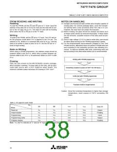
(4) For the programmable microcomputer (shipped in One Time
PROM version), Mitsubishi does not perform PROM write test
and screening in the assembly process and following pro-
cesses. To improve reliability after write, performing write and
test according to the flow below before use is recommended.
Note on Writing
When using a PROM programmer, the address range should be
between 400016 and 7FFF16. When data is written between ad-
dresses 000016 and 7FFF16, fill addresses 000016 to 3FFF16 with
FF16.
Writing with PROM programmer
Screening (Caution) (Leave at 150°C for 40 hours.)
Verify test with PROM programmer
Erasing
Data can only erased on the M37478E8SS ceramic package,
which includes a window. To erase data on this chip, use an ultra-
violet light source with a 2537 Angstrom wave length. The
2
minimum radiation power necessary for erasing is 15W·s/cm .
Function check in target device
Caution : Since the screening temperature is higher than storage
temperature, never expose to 150°C exceeding 100
hours.
Table 3. I/O signal in each mode
Pin
__
CE
__
OE
VPP
VCC
Data I/O
Mode
Read-out
VIL
VIL
VIL
VIH
VIH
VIL
VIH
VIH
VIL
VIH
VCC
VCC
VPP
VPP
VPP
VCC
VCC
VCC
VCC
VCC
Output
Floating
Input
Output disable
Programming
Programming verify
Program disable
Output
Floating
Note : VIL and VIH indicate an “L” and an “H” input voltage, respectively.
38

 MITSUBISHI [ Mitsubishi Group ]