MITSUBISHI MICROCOMPUTERS
7477/7478 GROUP
SINGLE-CHIP 8-BIT CMOS MICROCOMPUTER
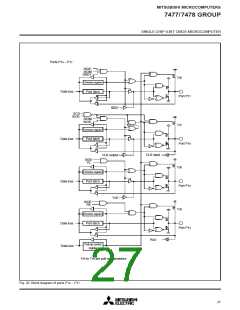
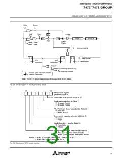
XCIN
XCOUT
X
IN
XOUT
1/2
T34M
0
1/8
Timer 3
Timer 4
1/2
CM
7
T34M
T34M
1
2
CM
CM
6
7
Internal clock φ
Q S
R
S Q
R
QQ S
R
Reset
STP instruction
WIT
instruction
STP
instruction
Reset
Interrupt disable flag I
Interrupt request
Select gate : At reset, shaded
side is connected.
Note : The 7477 group does not have X CIN input and XCOUT output.
Fig. 27 Block diagram of clock generating circuit
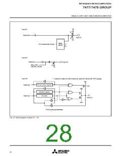
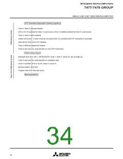
b7
b0
CPU mode register
(Address 00FB16
)
These bits must always be set to “0”.
Stack page selection bit (Note 1)
0 : In page 0 area
1 : In page 1 area
P5
0 : P5
0
, P5
1
/XCIN, XCOUT selection bit (Note 2)
, P5
0
1
1 : XCIN, XCOUT
XCOUT drive capacity selection bit (Note 2)
0 : Low
1 : High
Clock (XIN-XOUT) stop bit (Note 2)
0 : Oscillates
1 : Stops
Internal system clock selection bit (Note 2)
0 : XIN-XOUT selected (normal mode)
1 : XCIN-XCOUT selected (low-speed mode)
Notes 1 : In the M37477M4, M37478M4, set this bit to “0”.
2 : In the 7477 group, set this bit to “0”.
Fig. 28 Structure of CPU mode register
31

 MITSUBISHI [ Mitsubishi Group ]