MITSUBISHI MICROCOMPUTERS
M37270MF-XXXSP
M37270EF-XXXSP, M37270EFSP
SINGLE-CHIP 8-BIT CMOS MICROCOMPUTER with CLOSED CAPTION DECODER
and ON-SCREEN DISPLAY CONTROLLER
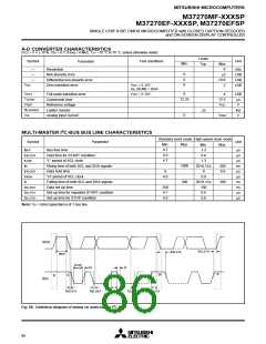
A-D CONVERTER CHARACTERISTICS
(VCC = 5 V ± 10 %, VSS = 0 V, f(XIN) = 8 MHz, T
a
= –10 °C to 70 °C, unless otherwise noted)
Limits
Typ.
Symbol
Test conditions
Unit
Parameter
Min.
Max.
8
—
—
—
Resolution
bits
LSB
LSB
LSB
0
0
0
±2
Non-linearity error
±0.9
2
Differential non-linearity error
Zero transition error
VOT
VCC = 5.12V
IOL (SUM) = 0mA
VFST
0
4
12.5
VCC
Full-scale transition error
Conversion time
VCC = 5.12V
LSB
µs
V
TCONV
VREF
12.25
Reference voltage
Ladder resistor
RLADDER
VIA
kΩ
V
25
0
VREF
Analog input current
2
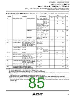
MULTI-MASTER I C-BUS BUS LINE CHARACTERISTICS
Standard clock mode High-speed clock mode
Symbol
Parameter
Unit
Min.
4.7
4.0
4.7
Max.
Min.
1.3
Max.
tBUF
Bus free time
µs
µs
µs
ns
µs
µs
ns
ns
µs
µs
tHD:STA
tLOW
Hold time for START condition
“L” period of SCL clock
0.6
1.3
1000
300
tR
Rising time of both SCL and SDA signals
Data hold time
20+0.1Cb
0
300
0.9
tHD:DAT
tHIGH
tF
0
“H” period of SCL clock
4.0
0.6
Falling time of both SCL and SDA signals
Data set-up time
20+0.1Cb
100
300
tSU:DAT
tSU:STA
tSU:STO
250
4.7
4.0
Set-up time for repeated START condition
Set-up time for STOP condition
0.6
0.6
Note: Cb = total capacitance of 1 bus line
SDA
tSU:STO
tHD:STA
tBUF
tLOW
tR
tF
p
Sr
p
S
SCL
tHD:STA
tHD:DAT
tHIGH
tSU:DAT
tSU:STA
2
Fig. 98. Definition diagram of timing on multi-master I C-BUS
86

 MITSUBISHI [ Mitsubishi Group ]