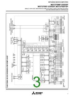
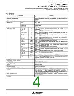
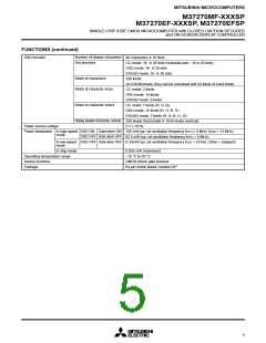
MITSUBISHI MICROCOMPUTERS
M37270MF-XXXSP
M37270EF-XXXSP, M37270EFSP
SINGLE-CHIP 8-BIT CMOS MICROCOMPUTER with CLOSED CAPTION DECODER
and ON-SCREEN DISPLAY CONTROLLER
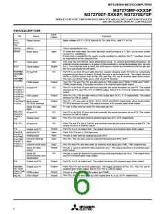
PIN DESCRIPTION (continued)
Output port
Output
Ports P60–P62, P65–P67 are a 6–bit output port. The output structure is N-channel open-
drain output.
P60–P62,
P65–P67
Input port
Input
Input
Ports P63 and P64 are 2-bit input port.
P63/OSC1/
XCIN,
P64/OSC2/
XCOUT
Clock input for OSD
Clock output for OSD
Sub-clock output
Sub-clock input
I/O for data slicer
P63 pin is also used as OSD clock input pin OSC1.
Output
Output
Input
P64 pin is also used as OSD clock output pin OSC2. The output structure is CMOS output.
P64 pin is also used as sub-clock output pin XCOUT. The output structure is CMOS output.
P63 pin is also used as sub-clock input pin XCIN.
CVIN
Input
Input composite video signal through a capacitor.
Input
VHOLD
RVCO
HLF
Connect a capacitor between VHOLD and VSS.
Connect a resistor between RVCO and VSS.
Connect a filter using of a capacitor and a resistor between HLF and VSS.
This is a horizontal synchronizing signal input for OSD.
This is a vertical synchronizing signal input for OSD.
Input
Input
HSYNC
VSYNC
HSYNC input
VSYNC input
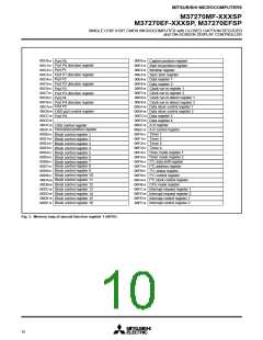
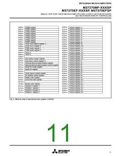
Note : As shown in the memory map (Figure 3), port P0 is accessed as a memory at address 00C016 of zero page. Port P0 has the port P0
direction register (address 00C116 of zero page) which can be used to program each bit as an input (“0”) or an output (“1”). The pins
programmed as “1” in the direction register are output pins. When pins are programmed as “0,” they are input pins. When pins are
programmed as output pins, the output data are written into the port latch and then output. When data is read from the output pins, the
output pin level is not read but the data of the port latch is read. This allows a previously-output value to be read correctly even if the
output “L” voltage has risen, for example, because a light emitting diode was directly driven. The input pins are in the floating state, so the
values of the pins can be read. When data is written into the input pin, it is written only into the port latch, while the pin remains in the
floating state.
7

 MITSUBISHI [ Mitsubishi Group ]