Mitsubishi microcomputers
M16C / 61 Group
SINGLE-CHIP 16-BIT CMOS MICROCOMPUTER
Serial I/O
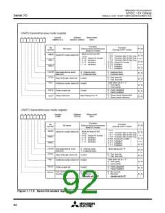
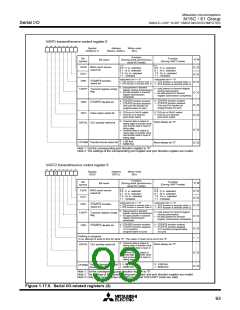
UARTi transmit/receive control register 0
b7 b6 b5 b4 b3 b2 b1 b0
Symbol
UiC0(i=0,1)
Address
03A416, 03AC16
When reset
0816
Function
(During clock synchronous
serial I/O mode)
Bit
symbol
Function
(During UART mode)
R W
Bit name
b1 b0
b1 b0
CLK0 BRG count source
select bit
0 0 : f1 is selected
0 1 : f8 is selected
1 0 : f32 is selected
1 1 : Inhibited
0 0 : f1 is selected
0 1 : f8 is selected
1 0 : f32 is selected
1 1 : Inhibited
CLK1
Valid when bit 4 = “0”
0 : CTS function is selected (Note 1)
1 : RTS function is selected (Note 2)
Valid when bit 4 = “0”
0 : CTS function is selected (Note 1)
1 : RTS function is selected (Note 2)
CRS
CTS/RTS function
select bit
0 : Data present in transmit
register (during transmission)
1 : No data present in transmit
register (transmission
0 : Data present in transmit register
(during transmission)
1 : No data present in transmit
register (transmission completed)
TXEPT Transmit register empty
flag
completed)
0 : CTS/RTS function enabled
1 : CTS/RTS function disabled
(P60 and P64 function as
programmable I/O port)
0 : CTS/RTS function enabled
1 : CTS/RTS function disabled
(P60 and P64 function as
programmable I/O port)
CRD
NCH
CTS/RTS disable bit
Data output select bit
0 : TXDi pin is CMOS output
1 : TXDi pin is N-channel
open-drain output
0: TXDi pin is CMOS output
1: TXDi pin is N-channel
open-drain output
0 : Transmit data is output at
falling edge of transfer clock
and receive data is input at
rising edge
Must always be “0”
CKPOL CLK polarity select bit
1 : Transmit data is output at
rising edge of transfer clock
and receive data is input at
falling edge
0 : LSB first
1 : MSB first
UFORM Transfer format select bit
Must always be “0”
Note 1: Set the corresponding port direction register to “0”.
Note 2: The settings of the corresponding port register and port direction register are invalid.
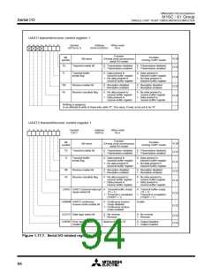
UART2 transmit/receive control register 0
b7 b6 b5 b4 b3 b2 b1 b0
Symbol
U2C0
Address
037C16
When reset
0816
Function
(During clock synchronous
serial I/O mode)
Bit
symbol
Function
(During UART mode)
R W
Bit name
b1 b0
b1 b0
CLK0
CLK1
BRG count source
select bit
0 0 : f1 is selected
0 1 : f8 is selected
1 0 : f32 is selected
1 1 : Inhibited
0 0 : f1 is selected
0 1 : f8 is selected
1 0 : f32 is selected
1 1 : Inhibited
Valid when bit 4 = “0”
0 : CTS function is selected (Note 1)
1 : RTS function is selected (Note 2)
Valid when bit 4 = “0”
0 : CTS function is selected (Note 1)
1 : RTS function is selected (Note 2)
CRS
CTS/RTS function
select bit
0 : Data present in transmit
register (during transmission)
1 : No data present in transmit
register (transmission
0 : Data present in transmit register
(during transmission)
1 : No data present in transmit
register (transmission completed)
TXEPT Transmit register empty
flag
completed)
0 : CTS/RTS function enabled
1 : CTS/RTS function disabled
(P73 functions
0 : CTS/RTS function enabled
1 : CTS/RTS function disabled
(P73 functions programmable
I/O port)
CRD
CTS/RTS disable bit
programmable I/O port)
0 : TXDi pin is CMOS output
1 : TXDi pin is N-channel
open-drain output
0: TXDi pin is CMOS output
1: TXDi pin is N-channel
open-drain output
Nothing is assigned.
In an attempt to write to this bit, write “0”. The value, if read, turns out to be “0”.
0 : Transmit data is output at
falling edge of transfer clock
and receive data is input at
rising edge
Must always be “0”
CKPOL CLK polarity select bit
1 : Transmit data is output at
rising edge of transfer clock
and receive data is input at
falling edge
0 : LSB first
1 : MSB first
0 : LSB first
1 : MSB first
Transfer format select bit
(Note 3)
UFORM
Note 1: Set the corresponding port direction register to “0”.
Note 2: The settings of the corresponding port register and port direction register are invalid.
Note 3: Only clock synchronous serial I/O mode and 8-bit UART mode are valid.
Figure 1.17.6. Serial I/O-related registers (3)
93

 MITSUBISHI [ Mitsubishi Group ]