SP8910
8
7
6
5
1
2
3
4
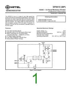
V
OUTPUT V
OUTPUT
OUTPUT
GND
CC
CC
INPUT
INPUT
GND
SP8910
MP8
Figure 2 Pin connections - top view
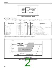
Electrical Characteristics
These characteristics are guaranteed by either production test or design over the following range of operating conditions
unless otherwise stated: TAMB = 240°C to 185°C, VCC = 4·75V to 5·25V
Value
Characteristic
Pin
Units
Conditions
Min. Typ. Max.
Supply current
1, 8
2, 3
2, 3
2, 3
2, 3
2, 3
2, 3
6, 7
6, 7
-
1·0
1·0
-
68
-
92
5·0
5·5
mA
Input frequency
Input frequency
Input sensitivity
Input sensitivity
Input overload
Input overload
Output voltage
Output power
GHz RMS sinewave
GHz RMS sinewave, TCASE = 255°C to 185°C
-
-
-
-
180 mVrms fIN = 1GHz and 4.2GHz
570 mVrms fIN = 5GHz
-
-
-
-
440
700
-
mVrms fIN = 1GHz and 3GHz
mVrms fIN = 5.0GHz and 3.8GHz
Vp-p Into 100Ω pullup resistor
0·25
218·0 29·0 24·0 dBm fIN = 1GHz and 5GHz (see note 1 )
NOTE
1. Measured into 50Ω measuring instrument in parallel with 100Ω pullup resistor. See Figure 5.
800
TESTED AS PER
TABLE OF
600
ELECTRICAL
CHARACTERISTICS
400
OPERATING WINDOW
200
1
2
3
4
5
6
7
FREQUENCY (GHz)
Figure3 Typical input sensitiviy (sinewave drive)
2

 MITEL [ MITEL NETWORKS CORPORATION ]