SL2015
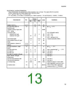
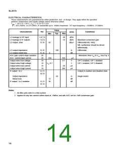
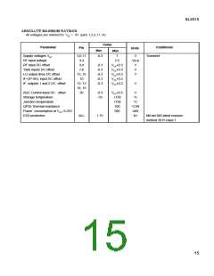
ELECTRICAL CHARACTERISTICS
These characteristics are guaranteed by either production test or design. They apply within the specified
ambient temperature and supply voltage unless otherwise stated.
TAMB = -20°C to + 80°C, VCC= + 4.75V to 5·25V.
IF = 403.25MHz or 479.5MHz; IF bandwidth up to 54MHz maximum. RF input frequency = 950MHz - 2150MHz.
Value
Characteristic
Pin
Conditions
Units
Typ
Max
Min
Supply Current, ICC
5,6,17
3,4
80
16
115
mA
dB
RF input Noise figure at
maximum gain
@ Tamb = 27°C
Variation of Noise Figure with
AGC setting
1
dB/dB
Conversion gain
AGC bandwidth 100kHz
AGC = 4.0V
minimum AGC gain
maximum AGC gain
-15
33
-5
dB
dB
25
AGC = 1.0V
AGC = self bias (2.4V)
Channel bandwidth 27MHz
Gain inband ripple
Gain variation across RF input
range
-0.25
-2
+0.25
+2
dB
dB
Gain imbalance between IF
outputs
12,13
18,19
3,4
-2
+2
dB
RF input impedance, single
ended
50
Ω
@ Tamb = 27°C
RF input return loss
RF input IP2
3,4
3,4
3,4
8
12
14
1
dB
Input unmatched @ Tamb = 27°C
See note 2
12
-1
dBm
dBm
RF input IP3
See note 2
RF input IP3 variation with gain
Input referred 1dB gain
compression
See Fig. 6
See Fig. 8
Two tone IM2 distortions with
Two tone IM3 distortions
LO tuning range
-31
-36
-33
-40
dBc
dBc
MHz
See note 2
See note 2
7,8
7,8
1250
2700
Maximum range of 1.4GHz within
band, application circuit as in Fig. 4.
SSB at 10kHz offset, application
circuit as in Fig. 4. ƒLO=2.63GHz
LO phase noise
-75
dBc/Hz
13

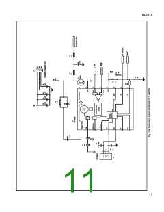
 MITEL [ MITEL NETWORKS CORPORATION ]
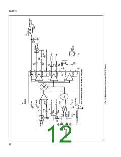