PDSP16510A MA
NnS > 2 X [nS + PK + D] for 50% overlapping
NnS > 4 X [nS + PK + D] for 75% overlapping
OPERATING MODES
The operating mode of the PDSP16510 is determined by
the condition of 16 bits in an internal Control Register. The
status of these bits is defined by the inputs present on the
AUX15:0pinswhentheDEFinputisactive.TheDEFinputcan
be a simple power on reset if the operating mode is fixed once
power is supplied. The AUX pins are also used to provide the
imaginary component of the complex input data. Thus, if
complex inputs are needed, the mode definition must be
implemented through a tri-state buffer which is only enabled
when DEF is active. The imaginary input data must be
disabled during this time.
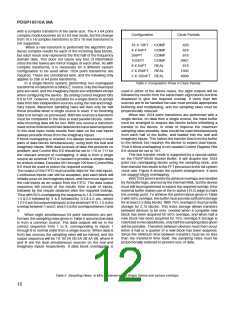
N is the number of devices, n is the transform size, S is the DIS
strobe period, P is the number of system clock periods given
inTable4, Kisthesystemclockperiod, andDisthetotaldump
time including 4 extra DOS periods as discussed previously.
The DIS and DOS periods are any value defined by the user,
down to the system clock period with the A grade part.
In this mode increasing the output clock frequency will
allow a greater continuous input rate. The provision of
separateDISandDOS pinsallowsthistobemechanized,and
the DOS frequency can be increased to that of the system
clock used internally. When the sum of the dump time (
including four extra DOS periods for output priming ) plus 12
system clock periods (the transform time variation caused by
input synchronization) is less than the load time, one device
will be guaranteed to have finished dumping before the next
one starts. The inverted DAV to DEN connection between
devices is then not needed, and all DEN inputs can be
grounded.
Table 6 lists the functionality of each of the bits in the
mode control register, and further explanations are as fol-
lows:-
BITS 2:0
These bits define one of 7 options for the sample size and
type of data. In the 1024 point options the device will assume
the non concurrent operating mode, regardless of whether a
single or multiple device system is specified. The internal
control logic will then ensure that data is loaded, transformed,
and dumped in sequential operations.
For other data set sizes, loading, transforming, and
dumping, can all occur simultaneously with a single device;
the actual overlap will be dependent on the relative occur-
rences of the INEN input. Only in Mode 1 can concurrent
operations be done with multiple devices.
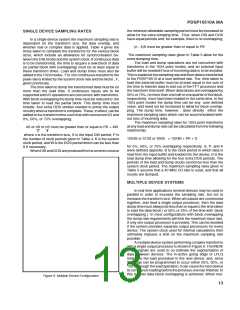
The LFLG transitions occur at the same times as Mode 1,
except that the double transition does not occur with multiple
concurrent transforms. Fig. 10 illustrates a timing sequence
with three devices. Real transforms still only use the real
inputs regardless of the amount of block overlapping.
MODE 3 (BITS 10:9 = 11)
MultipledeviceMode3isprovidedinordertoimprovethe
performancewhenblockoverlappingisneeded,andseparate
output processors are provided. In this mode transfers in and
out of the device are never concurrent with transform opera-
tions. The device will actually load extra data such that the
required data to perform two overlapped transforms is stored
internally. TheamountofinternalRAMprohibitstheuseofthis
mode when performing overlapped 1024 point transforms.
LFLG will go in-active after a normal data block have been
loaded, regardless of the overlap selected. The device, how-
ever, continues to load more data. Thus, for example, in the 4
x 64 mode, five 64 point blocks will be loaded. This technique
allows each device in the system to complete two or four
overlapped transforms (depending on the amount of overlap)
before any new data is needed. When doing a straightforward
256 point transform the device will load 256 + 128 data points.
The full benefits are only obtained if more than one output
processor is provided, but an extra processor is not always
necessary for every device. Sampling rates up to the system
clock rate are possible. The equations defining the sampling
rates become:
BIT 3
This bit determines the number of right shifts built into the
data path. In either condition only two right shifts occur during
thefirstpass.Ifthebitisreset,threeshiftsoccurinsubsequent
passesandtheblockfloatingpointschemeallowsuptofifteen
compensating left shifts. If it is set, two shifts occur in every
pass and overflow is possible. This is indicated by reducing
the number of compensating left shifts to fourteen, and using
scale tag value fifteen to indicate that overflow has occurred.
BITS 5:4
These bits define the choice of window operator. If other
windows are needed they must be applied externally. The
fourth option is used to specify the inverse transform, which
does not require the use of a window operator. When 16 x 16
complex transforms are specified by Bits 2:0, only the rectan-
gular window can be used. The use of any of the other options
will cause the device to enter an internal test mode.
BITS 8:6
These bits define 0%, 50%, or 75% data block overlap-
ping, and the division factor on the DIS input. Overlapping
must not be specified with 16 x 16 complex transforms.
Two decodes allow the DIS input to be divided by two or four,
when 50% and 75% overlapping is respectively needed.
These options allow the DOS and DIS input pins to be still
supplied from a common source, even though the output rate
mustbefasterthantheinputrate.Thefrequencyofthissource
would be dictated by the output rate requirement, with the
input rate internally reduced by the correct amount.
Special decodes are provided to support real only trans-
forms from dual sources, using both the real and auxiliary
(N - 1)L > 2PK + 2D for 50% overlaps
(N - 1)L > 4PK + 4D for 75% overlaps
where L is the time needed to load a normal block of data but
not including the extra data, P is the number of system clock
periods given in Table 4, K is the system clock period, and D
is the total dump time including 4 extra DOS periods.
When real transforms are to be performed on single
sourced data, an external FIFO is needed to provide pairs of
data blocks. These are loaded simultaneously into the real
and imaginary inputs. See the section on real transforms.
16

 MITEL [ MITEL NETWORKS CORPORATION ]