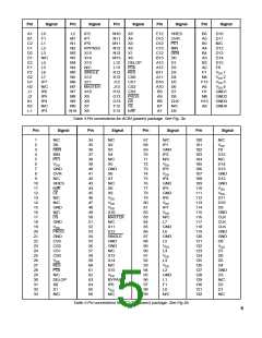
Signal
IP7:0
Type
Input
Description
Pixel data input to the first line delay (most significant byte in 16-bit mode).
L7:0
I/O
Pixel data input to the second group of line delays. (least significant byte in 16-bit mode). Alterna-
tively an output from the last line delay when the appropriate mode bit is set.
BYPASS
HRES
Input
Input
The first line delay in the first group is bypassed when this input is high. No internal pullup resistor.
Resets the line delay address pointers when high. Normally the composite sync signal in real time
applications. In non real time systems it defines a frame store update period, when low.
X15:0
D15:0
PC1
Dual
function
Address/data connections from a Master or Single device to the external coefficient source,
with X15 defining EPROM or Host support. Otherwise they provide the expansion data input.
Output
Output
Input
Signed 16-bit scaled data or multiplexed 32-bit intermediate data. During intermediate transfers the
most significant half is valid when the clock is low, and the least significant half when clock is high.
During programming a Master device outputs a timing strobe on this pin. This is passed down
the chain in a multiple device system, using the PC0 input on the next device.
PC0
This pin is used in conjunction with
in multiple device systems. It terminates the write strobe
PC1
from a Master device which is EPROM supported.
DELOP
DS
Output
I/O
This output provides a version of the HRES input which has been delayed by an amount defined by
the user.
The data strobe from a host computer, active low. This pin will be an output from an EPROM
supported Master device which provides strobes to the remaining devices.
CE
Input
An active low enable which is internally gated with
and
to perform reads or writes to the
DS
R/W
internal registers. In a Single or Master device, which is supported from an EPROM, the
bottom 72 addresses are always used and is not needed. can then be used to initiate a
CE
new register load sequence after the power on load sequence.
CE
R/W
Input
I/O
Read / not write line from the host CPU. When an EPROM is used this pin should be tied low.
PROG
This pin is normally an input which signifies that registers are to be changed or examined. It is,
however, an output from an EPROM supported Single or Master device indicating to the rest
of the system that registers are being updated.
CLK
BIN
Input
Clock. All events are triggered on the rising edge of CLK, except the latching of least significant
expansion inputs . Internally the clock can be multiplied by two or four in order to increase the
effective number of multipliers.
Output
This output indicates the result from the internal comparison. A high value indicates that the pixel
was greater than the internal threshold. The output is only valid from the last device in a chain.
OVR
Output
Input
Input
Input
When high this output indicates that there has been a gain control overflow.
Active low power on reset signal.
RES
SINGLE
MASTER
Tied to ground to indicate a Single device system. Internal pullup resistor.
Tied to ground to indicate the Master device in a multiple device system. Must be left open circuit
in a Single device system. Internal pullup resistor.
Input
OEN
Output enable signal. Active low.
CS3:0
Outputs
Four address bits from a Master specifying one of sixteen devices in a multiple device system.
Must be externally decoded to provide chip enables for the additional devices.
F1:0
Outputs
These bits indicate the field selection given by the gain control auto select logic. The same coding
as that used for Control Register bits C5:4 is used.
VDD
Power
Power
15V supply. All VDD pins must be connected.
GND
0V supply. All GND pins must be connected.
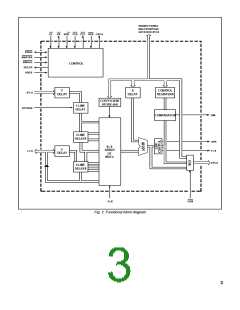
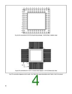
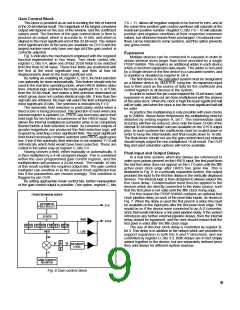
Table 3 Signal descriptions
2

 MITEL [ MITEL NETWORKS CORPORATION ]