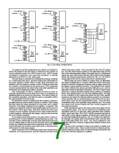
The data from the last device in a horizontal row of convolvers
feeds the expansion input of the first device in the next row. This
is shown in Fig. 7. With this arrangement, the position of the partial
window as illustrated, is the inverse of its vertical position on a
normal TV screen. Thus the top left hand device corresponds to
the bottom left hand portion of the complete window.
The output from the last device in the row is delayed with
respect to the original data input by an amount given by the
formula;
Hex address
Function
Mode Reg A
Mode Reg B
Mode Reg C
Mode Reg D
Comparator LSB
Comparator MSB
Scale value
Pixels/line LSB
Pixels/line MSB
C0-C15
00
01
02
03
04
05
06
07
08
40-4F
50-5F
60-6F
70-7F
09-3F
DELAY = 41S(N21), where N is the number of devices in a
row and S is the partial window width, i.e. 4 or 8.
The internal convolver sums, in each of the devices in the next
row, must be delayed by this amount before they are added to
results from the previous row. This is more conveniently achieved
by delaying data going into the line stores. The required cumula-
tive delay with respect to the first horizontal stripe is then
automatically obtained when more than two rows of devices are
needed.
C16-C31
C32-C47
C48-C63
Unused
Register D, bits 3:2 are used to define one of four delay
options. These delays have been selected to support systems
needing from two to eight devices and are described in the
applications section.
Table 5 Internal register addressing
Pipeline delay
Data size
Window size
8
8
8
15
16
434
834
838
434
834
34
30
26
28
26
Coefficients
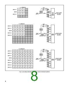
Sixty-four coefficients are stored internally and must be
initially loaded from an external source. Table 5 gives the
coefficient addresses within a device, with coefficient C0 speci-
fied by the least significant address and C63 by the most
significant address. Fig. 9 shows the physical window position
within the device that is allocated to each coefficient in the various
modes of operation. Horizontally the coefficient positions corre-
spond to the convolution process as if it were observed on a
viewing screen, i.e. the left hand pixel is multiplied with C0. In the
vertical direction the lines of coefficients are inverted with respect
to a visual screen, i.e. the line starting with C0 is actually at the
bottom of the visualized window.
The coefficients may be provided from a Host CPU using
conventional addressing, a read/not write line, data strobe, and
a chip enable. Alternatively, in stand alone systems, an EPROM
may be used. A single EPROM can support up to 16 devices with
no additional hardware.
Table 6 Pipeline delays
Total Pipeline Delay
The total pipeline delay is dependent on the device configu-
ration and the number of devices in the system. Table 6 gives the
delays obtained with the various single device configurations
when the gain control is used. These delays are the internal
processing delays and do not include the delays needed to move
a given size window completely into a field of interest. When
multiple devices are needed, additional delays are produced
which must be calculated for the particular application. These
delays are discussed in the applications section.
The PDSP16488A contains facilities for outputting a delayed
version of HRES (DELOP) to match any processing delay.
Register C. bits 3:1 allow this delay to be selected from any value
between 29 and 92 pixel clocks as detailed in Table 9.
When windows are to be fabricated which are smaller than
the maximum size that the device will provide in the required
configuration, then the areas which are not to be used must
contain zero coefficients. The pipeline delay will then be that of a
completely filled window.
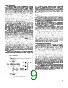
ACTIVE LINE PERIOD
tRSU
ASYNCHRONOUS BACK EDGE
HRES
(sync)
2
3
4
5
6
7
8
1
2
6
7
CLK
FIRST
PIXEL
VALID
(REG B3
SET)
FIRST
PIXEL
FROM
LINE
STORE
VALID
LAST2
PIXELS
INTER-
NALLY
LINE STORE
WRITES INHIBITED
STORED
Fig.8 Pixel input delays
11

 MITEL [ MITEL NETWORKS CORPORATION ]