PDSP16116
Complex Conjugation
SYSTEM FEATURES
Many algorithms using complex arithmetic require conjuga-
tion of complex data stream. This operation has traditionally re-
quired an additional ALU to multiply the imaginary component
by -1. The PDSP16116 eliminates this requirement by offering
on-chip complex conjugation of either of the two incoming com-
plex data words with no loss in throughput.
The PDSP16116 has a number of features tailored for sys-
tem applications.
(21)3(21) Trap
In multiply operations using two’s complement fractional no-
tation, the (21)3(21) operation forms an invalid result because
11 is not representable in the fractional number range. The
PDSP16116 eliminates this problem by trapping the (21)3(21)
operation and forcing the multiplier result to become the most
positive representable number.
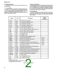
Easy Interfacing
As with all PDSP family members the PDSP16116 has reg-
istered l/O for data and control. Data inputs have independent
clock enables and data outputs have independent three state
output enables.
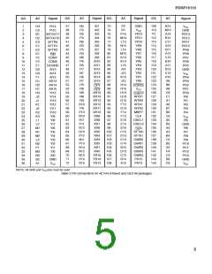
Normal
mode
Signal
Type
Description
configuration
XR15:0
Input
16-bit input for real X data
Xl15:0
Input
16-bit input for imaginary X data
16-bit input for real Y data
YR15:0
Yl15:0
Input
Input
16-bit input for imaginary Y data
16-bit output for real P data
PR15:0
Pl15:0
Output
Output
Input
16-bit output for imaginary P data
Clock; new data is loaded on rising edge of CLK
Clock, enable X-port input register
Clock, enable Y-port input register
Conjugate X data
CLK
CEX
Input
CEY
Input
CONX
Input
CONY
Input
Conjugate Y data
ROUND
MBFP
Input
Rounds the real and imaginary results
Mode select (BFP/Normal)
Input
Tie low
Tie low
Tie low
Tie low
Tie low
Tie low
SOBFP
EOPSS
AR15:1 3
Al15:1 3
WTA1:0
WTB1:0
WTOUT1:0
SFTA1:0
SFTR2:0
GWR4:0
OSEL1:0
OER, OEI
VDD
Input
Start of BFP operations (see Note 1)
End of pass (See Note 1)
Input
Input
3 MSBs from real part of A-word (See Note 1)
3 MSBs from imaginary part of A-word (See Note 1)
Word tag from A-word
Input
Input
Input
Word tag from B-word/shift control (See Note 2)
Word tag output (See Note 1)
Output
Output
Output
Output
Input
Shift control for A-word / overflow flag (See Note 2)
Shift control for accumulator result (See Note 1)
Global weighting register contents (See Note 1)
Selects the desired output configuration
Output enables
Input
Power
Power
15V Supply (See Note 3)
GND
0V Supply (See Note 3)
NOTES
1. Used only in BFP mode
2. Performs different functions in BFP/Normal modes
3. All supply pins must be connected
Table 1 Signal descriptions
2

 MITEL [ MITEL NETWORKS CORPORATION ]