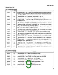
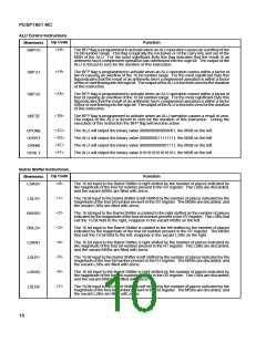
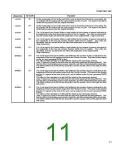
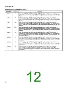
PDSP1601 MC
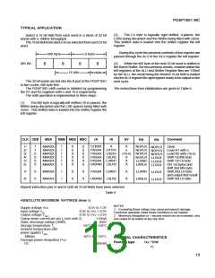
TYPICAL APPLICATION
(2)
The LS byte is logically right shifted, n-places, the
Select a 16 bit field from each word in a block of 32 bit
words with a 10MHz throughput.
The 16 bit field indicated is to be selected from each 32 bit
word.
LSBs being discarded and the MSBs being filled with zeros.
This shifted data is loaded into the shifter register file left
register.
During this cycle the previous contents of this register are
passed through the ALU to the ALU register file left register.
MS Byte
LS Byte
MS Bit
(3)
While the MS byte of the next 32 bit word is shifted in
8
8
8
8
the Barrel Shifter, the two previous results, resident within the
left registers of the ALU and Shifter Register files are 'ORed'
by the ALU, the result being the desired 16 bit field is loaded
intotheALUregisterfilerightregisterreadytobeoutputonthe
next cycle.
16 bits
nbits
The 32 bit words are fed into the B port of the PDSP1601
in two cycles, MS byte first.
The PDSP1601 shift control is initiated by programming
the R1 and R2 registers with n and 16-n respectively.
The shift operation is implemented in three steps:-
The instructions from initialisation are given in Table 6.
(1)
The MS byte is logically left shifted (16-n) places, the
MSBs being discarded and the LSB spaces being filled with
zeros. This shifted data is loaded into the shifter register file
left register.
IA
IS
CLK CEB
MSA
MSB MSS MSC
SV
Comment
RA
RS
CLRXX
X
1/
2/
3/
4/
5/
6/
1
1
0
0
0
0
MARSX
MARSX
MARSX
MARSX
MARSX
MARAX
1
1
1
1
1
1
0
0
0
0
0
0
0
0
0
0
0
0
X
Clear
NOPLR
NOPLR
NOPLR
NOPLR
LLRRR
LRRLR
NOPLR
NOPLR
NOPLR
LLRLR
LLRLR
LLRLR
PASXA LR1SV
PASXA LR2SV
PASXA LSLR2
PASXA LSRR1
ORXAB LSLR2
n
(16-n)
X
X
X
Load R1 with n
Load R2 with (16-n)
Shift 1st MS byte
Shift 1st LS byte
OR 1st bytes and
shift 2nd MS byte
Shift 2nd LS byte
and output first result
Shift 3rd LS byte
PASXA LSRR1
ORXAB LSLR2
7/
8/
0
0
MARSX
MARAX
1
1
0
0
0
0
X
X
LLRRR
LRRLR
LLRLR
LLRLR
Repeat instruction pair 5/ and 6/ until all 16 bit fields have been selected.
Table 6
ABSOLUTE MAXIMUM RATINGS (Note 1)
NOTES
Supply voltage Vcc
Input voltage VIN
Output voltage VOUT
Clamp diode current per pin IK (see note 2)
Static discharge voltage (HMB)
Storage temperature TS
Ambient temperature with
power applied Tamb
-0.5V to 7.0V
-0.9V to Vcc + 0.9V
-0.9V to Vcc + 0.9V
1. Exceeding these ratings may cause permanent damage.
Functional operation under these conditions is not implied.
2. Maximum dissipation or 1 second should not be exceeded, only
one output to be tested at any one time.
±18mA
500V
-65°C to +150°C
Military
-40°C to +125°C
THERMAL CHARACTERISTICS
Package power dissipation PTOT
GC
Package type
ΘJC °C/W
1000mW
GC
12
13

 MITEL [ MITEL NETWORKS CORPORATION ]