MT8986
Pin Description (continued)
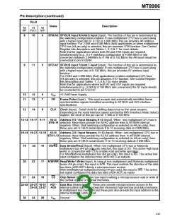
Pin #
Name
Description
40
44
44
DIP PLCC QFP
8 10 4
STi6/A6 ST-BUS Input 6/Addr.6 input (Input). The function of this pin is determined by
the switching configuration enabled. If non-multiplexed CPU bus is used along
with a higher input rate of 8.192 or 4.096 Mb/s, this pin provides A6 address
input function. For 2.048 and 4.096 Mb/s (8x4) applications or when multiplexed
CPU bus (44 pin only) is selected, this pin assumes STi6 function. See Control
Register bits description and Tables 1, 2, 6 & 7 for more details.
Note that for applications where both A6 and STi6 inputs are required
simultaneously (e.g., 8 x 4 switching configuration at 4.096 Mb/s or rate
conversion between 2.048Mb/s to 4.196 or 8.192 Mb/s) the A6 input should be
connected to pin STo6/A6.
9
11
5
STi7/A7 ST-BUS Input 7/Addr.7 input (Input): The function of this pin is determined by
the switching configuration enabled. If non-multiplexed CPU bus is used along
with a higher input rate of 8.192 Mb/s, this pin provides A7 address input
function.
For 2.048 and 4.096 Mb/s (8x4) applications or when multiplexed CPU bus
(44 pin only) is selected, this pin assumes STi7 function. See Control Register
bits description and Tables 1, 2, 6 & 7 for more details.
Note that for applications where both A7 and STi7 inputs are required
simultaneously (e.g., 2.048 to 8.192 Mb/s rate conversion) the A7 input should
be connected to pin STo7/A7.
10
11
12
13
6
7
VDD
FR
+5 Volt Power Supply.
Frame Pulse (Input). This input accepts and automatically identifies frame
synchronization signals formatted according to ST-BUS and GCI interface
specifications.
12
14
8
CLK Clock (Input). Serial clock for shifting data in/out on the serial streams.
Depending on the serial interface speed selected by IMS (Interface Mode Select)
register, the clock at this pin can be 4.096 or 8.192 MHz.
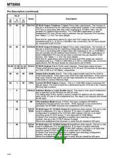
13-15 15-17 9-11
A0-2/ Address 0-2 / Input Streams 8-10 (Input). When non-multiplexed CPU bus is
STi8-10 selected, these lines provide the A0-A2 address lines to MT8986 internal
registers. When 16x8 switching configuration is selected (in 44 pin only), then
these pins are ST-BUS serial inputs 8 to 10 receiving data at 2.048 Mb/s.
16-18 19-21 13-15 A3-5/ Address 3-5 / Input Streams 11-13 (Input). When non-multiplexed CPU bus is
STi11-13 selected, these lines provide the A3-A5 address lines to MT8986 internal
registers. When 16x8 switching configuration is selected (in 44 pin only), then
these pins are ST-BUS serial inputs 11 to 13 receiving data at 2.048 Mb/s.
19
20
21
22
23
24
16
DS/RD Data Strobe/Read (Input). When non-multiplexed CPU bus or Motorola
multiplexed bus (44 pin only) are selected, this input is DS. This active high input
works in conjunction with CS to enable read and write operation.
For Intel/National multiplexed bus (44 pin only), this input is RD. This active low
input configures the data bus lines (AD0-AD7) as outputs.
17 R/W\WR Read/Write \ Write (Input). In case of non-multiplexed and Motorola multiplexed
buses (44 pin only), this input is R/W. This input controls the direction of the data
bus lines (AD0-AD7) during a microprocessor access.
With Intel/National multiplexed timing (44 pin only), this input is WR. This active
low signal configures the data bus lines (AD0-AD7) as inputs.
18
CS
Chip Select (Input). Active low input enabling a microprocessor read or write of
the control register or internal memories.
22-29 25-27 19-21 AD7- Data Bus (Bidirectional): These pins provide microprocessor access to the
29-33 23-27
AD0 internal control registers, connection memories high and low and data memories.
In multiplexed bus mode (44 pin) these pins also provide the input address to the
internal Address Latch circuit.
30
34
28
VSS
Ground.
2-65

 MITEL [ MITEL NETWORKS CORPORATION ]