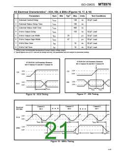
ISO-CMOS MT8976
compatible equipment (see ANSI T1.102 and AT & T
Technical Advisory #34). On the receive side the
bipolar line signal is converted into a unipolar
format by the line receiver circuit. The resulting
split phase signals are input at the RxA and RxB pins
on the MT8976. The signals are combined together
to produce a composite return to zero signal, which
is clocked into the device at RxD. An uncommitted
nand gate in the MT8940/41 can be used for this
purpose.
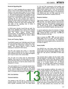
the STPA transmit RAM’s Tx0, Tx1, while status
information is read at receive RAM Rx0. In addition,
interrupts can be set up to notify the system in case
of slips, loss of sync, alarms, violations, etc.
Mitel also manufactures a thick film hybrid device,
the MH89760/760B, which incorporates the line
driver, receiver and clock extractor circuitry.
A
second SIP hybrid, the MH89761, provides the
necessary equalization circuitry to condition the
signal for transmission up to 655 feet over 22 AWG
twisted pair.
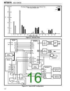
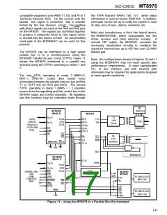
The MT8976 can be interfaced to a high speed
parallel bus or to a microprocessor using the
MT8920B Parallel Access Circuit (STPA). Figure 11
shows the MT8976 interfaced to a parallel bus
structure using two STPA‘s operating in modes 1 and
2.
Note: the configurations shown in Figures 10 and 11
using the MT8940/41 may not meet specific jitter
performance requirements. A more sophisticated
PLL or line interface unit with transmit jitter
attenuator may be required for applications designed
to meet specific standards.
The first STPA operating in mode 2 (MMS=0,
MS1=1, 24/32=0), routes data and/or voice
information between the parallel telecom bus and the
T1 or CEPT link via DSTi and DSTo. The second
STPA, operating in mode 1 (MMS = 1 ) provides
access from the signalling and link control bus to the
MT8976 status and control channels. All signalling
and link functions may be controlled easily through
DIP
MT8920B
(Mode 2)
SWITCH
MT8976
D0-D7
Tx
Line
HIGH
SPEED
PARALLEL
TELECOM
BUS
DSTi
STo0
STi0
STo1
TxA
TxB
EQU
A0-A5
DSTo
Driver
CSTi0
CSTo
CSTi1
CS
R/W
OE
MH89761
C4i
F0i
Rx
Line
F0i
RxA
RxB
•
•
C2i
•
Receiver
MMS MS1 24/32
C1.5i
+5V
RxD
•
MT8940/41
MT8920B
(Mode 1)
E1.5i
E8Ko
D0-D7
STo0
A0-A5
STi0
Clock
Extractor
STo1
CS
DS
R/W
SIGNALLING
and
MT8940/
MT8941
1.544
MHz
LINK
12.355/12.352
MHz Osc.
CVb
CONTROL
BUS
DTACK
IRQ
lACK
C4i
F0i
•
F0i
•
C2o
MMS
+5V
F0b
C4b
C8Kb
•
16.388/16.384
MHz Osc.
Figure 11 - Using the MT8976 in a Parallel Bus Environment
4-45

 MITEL [ MITEL NETWORKS CORPORATION ]