ISO-CMOS MT8952B
timeslot of the incoming ST-BUS (CDSTi) during the
Internal Timing Mode of the Protocol Controller.
When the data is detected in the transmit FIFO, the
protocol controller will proceed in one of the following
ways:
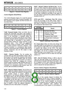
RESET
If the transmitter is in idle state, the present byte of
eight ONEs being transmitted is completed and
then followed by a start flag and subsequently
the data in the transmit FIFO is transmitted.
When the MT8952B is reset by a low going pulse on
the RST pin or by setting (logic high) the RST bit in
the Timing Control Register, the device is put into the
following state:
If the transmitter is in the interframe time fill state,
the flag presently being transmitted is finished
and then another start flag is transmitted before
transmitting the data from the transmit FIFO.
a) All bits in the Timing Control Register are cleared
(logic 0) by an external reset. An internal reset
clears all bits except the RST bit.
If the transmitter is in go ahead state, it continues to
be in that state even after the data is loaded into
the FIFO. Only when the IFTF bits are set to
choose something other than go ahead will the
data be transmitted.
b) All bits in the Interrupt Enable Register are
cleared (logic 0).
c) All bits in the Control Register are cleared (logic
0).
If the transmitter is in transparent data transfer state,
the protocol functions are disabled and the data
in the transmit FIFO is transmitted on CDSTo.
d) All bits in the Interrupt Register are cleared (logic
0).
e) All bits in the General Status Register are cleared
(logic 0) except for the two least significant bits.
To indicate that the particular byte is the last byte of
the packet, the EOP bit in the Control Register must
be set before the last byte is written into the transmit
FIFO. The EOP bit is cleared automatically when the
data byte is written to the FIFO. After the
transmission of the last byte in the packet, the frame
check sequence (16 bits) is sent followed by a
closing flag. If there is any more data in the transmit
FIFO, another flag is transmitted followed by the new
data. In case of no data in the FIFO, the transmitter
assumes the selected link channel state. During the
transmission of either the data or the frame check
sequence, the Protocol Controller checks the
transmitted information on a bit by bit basis and
inserts a ZERO after every sequence of five
consecutive ONEs.
f) Receive and Transmit Registers are cleared and
the FIFO Status Register reflects their state
accordingly.
g) The WD output is reset low by an external reset
but is not affected by an internal reset.
h) The Transmitter and the Receiver are disabled.
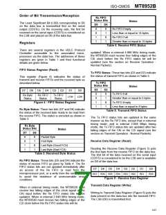
Transmit Operation
After a reset, which the external circuitry should
provide upon power up, the transmit section is
disabled. Before enabling this section, the timing
should be set up. On reset, the serial port is set to
External Timing Mode. In case this is not desired, the
Timing Control Register should be written to with the
appropriate data. Once in the correct timing mode,
the Transmit Enable (TxEN) bit in the Control
Register can be set. Now that the transmitter is
enabled it will be in the Idle channel state. If any
other channel state or the transparent data transfer
facility is required, the IFTF bits in the Control
Register should be set accordingly.
Transmit FIFO Full:
When the Transmit FIFO is full, this state is indicated
by the Transmit FIFO status bits in the FIFO Status
Register. These bits do not change state for two bit
periods after an access of the FIFO from either the
serial port or the microprocessor port. The bit period
is determined by the CKi signal frequency. If the bus
cycle of the controlling microprocessor is much
shorter than the bit period, the Transmit FIFO status
bits may not be updated in time for the next
microprocessor read of the FIFO Status Register.
Normal Packets:
To start a packet, the data is written into the transmit
FIFO starting with the address field. All the data
must be written to the FIFO in a bytewide manner.
To make sure that the microprocessor does not
overwrite the Tx FIFO, if over four bytes of
information have been written to the Tx FIFO, the
3-71

 MITEL [ MITEL NETWORKS CORPORATION ]