SL1711
I & Q baseband outputs
I2C Bus connections
The board is provided with an RJ11 I2C bus connector
which feeds directly to the SP5611 synthesiser.
The SL1711 offers a greatly improved drive capability over
the SL1710 and as such is much less sensitive to the load
conditions.
It is still important however to carefully balance the loads
presented to the SL1711 to ensure no differential gain or
phasedegradationisintroducedbytheloadcircuits, whichwill
also include effects due to track striplines etc.
This connects to a standard 6-way connector cable which
is supplied with the I2C/3-wire bus interface box.
Input and Output connections
For demonstration purposes the output is unsuitable for
connection via co-axial cables to standard test equipment,
where such equipment is normally 50 Ω or highly capacitive.
To overcome this problem the outputs of the SL1711 are
therefore buffered through emitter followers which are
optimisedtodrive50Ω loadswithoutappreciabledegradation
in the SL1711 performance. These buffer stages are
selectable so enabling the outputs to be loaded directly for
interfacing direct with an ADC via a low capacitive link.
In most applications the SL1711 will normally interface
direct into the ADC converter such as the VP216, which will
present a >1 kΩ low capacitive load, though it can interface
with lower impedances if desired.
The board is provided with the following connectors:
A) IF I/P SMA connector SK1 which is AC coupled to the
RF input of the SL1711.
B) I CH OUT SK2 and Q CH OUT (SK3) which provide
either a buffered or direct baseband output signal from
the SL1711 (depending on which way the links LK1
and LK2 are set). The output buffers should be used
when driving 50Ω test equipment or co-axial lines.
The output is optimised for typical drive levels of 760
mVp-p and the onset of clipping is typically > 1.5V.
Links and Switches
The board is provided with the following:
VCO DISABLE switch
Care must be taken with system design to ensure that the
I and Q baseband output signals never exceed 1.2V pk-pk.
Any gross distortion in the output waveform caused by
overdriving the output stages will compromise the system
performance.
This disables the VCO of the SL1711. It does NOT power
down the chip.
Device performance characteristics can only be
guaranteed if the device is operated below the onset of
clipping.
AGC ADJUST potentiometer
The potentiometer sets the AGC input voltage of the
SL1711 which controls the gain of the chip. TP1 is provided as
a means of monitoring the AGC voltage.
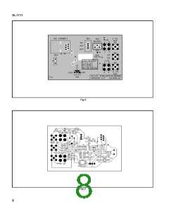
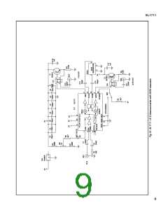
SL1711 Evaluation Board
This board has been created to show the operation of the
SL1711 I/Q downconverter.
LK1 and LK2
It does not attempt to simulate a real system, since in
practice the 479.5MHz IF oscillator on the SL1711and the
60MHz clock on the subsequent ADC would be controlled via
the baseband IQ demodulator chip such as the VP305 which
follows the dual channel ADC. For simplicity, the VCO is
locked using Mitel Semiconductor SP5611 synthesiser, con-
trolled via an I2C bus.
These are links which may be placed either vertically or
horizontally to connect the outputs of the SL1711 either
directly or via buffers to the SMA output connectors of the
board.
If the links are placed vertically 1-2 and 3- the outputs are
connected directly.
If the links are placed horizontally 1-3 and 2- the ouputs are
connected via buffers.
For full evaluation, 30V and 5V supplies are necessary.
Supplies
The board must be provided with the following supplies:
A) 5V for the SL1711 and SP5611 and 30V for the
varactor line.
The supply connector is a 3 pin 0.1" pitch pin header. The
centre pin of the connector is GND.
Outputs driven into hard clipping can exhibit amplitude
decline.AGCloopsshouldbedesignedtotakeaccountofthis.
12

 MITEL [ MITEL NETWORKS CORPORATION ]