SL1711
APPLICATION NOTES
These application notes should be read in conjunction with
circuit diagrams contained in Fig. 7 and 10, and a
recommended front end tuner solution contained in Fig. 13.
These boards have been designed to demonstrate
performance and to allow for initial evaluation of the SL1711.
These enable the VCO frequency to be synthesised by a PLL
frequency synthesiser; on the demo board an SP5611 is used
for this function however in a real application this function will
be provided by the QPSK demodulator function contained in
for example the VP305
It is recommended that the prescaler outputs are loaded
symmetrically to balance radiation effects.
Varator Tuned Oscillator
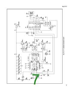
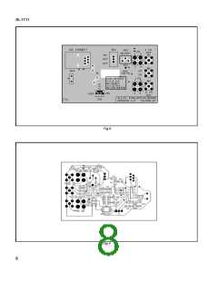
Refer to Fig. 7 circuit diagram and Figs. 11 and 12 PCB
layout.
Saw Resonator Oscillator
This application uses a synthesised VCO with a tuning
range of 460 MHz to 500 MHz. The surface mount inductor L1
is 12 nH. The VCO frequency is controlled by the SP5611
synthesiserwhichisprogrammedviaanI2Cbus. TheRFinput
to the synthesiser is from the SL1711 prescaler outputs
coupled via RF inductors L3 and L4.
For functional checking the VCO can be tuned by
physically shorting the base of transistor T3 to ground and
then adjusting the +30 volt supply to tune the VCO. Under
these conditions, due to the unlocked state of the LO, the
board WILL NOT BE representative of locked gain and phase
match or phase noise performance.
In real applications such the VCO control voltage will be
provided by the QPSK demodulator circuit, such as the
VP305. This circuit provides a line voltage to align the
reference LO in the 1711 in both frequency and phase to the
centre of the modulation bandwidth, normally 402.75 or 479.5
MHz.
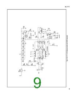
Refer to Fig. 10 circuit diagram and Figs 11 and 12 PCB
layout.
In the standard application the oscillator uses a varactor
diode tuned tank circuit which allows fine tuning of the
oscillator frequency via a voltage control line. This control
voltage is usually derived from the QPSK/FEC decoder
VP305/VP306
Certain applications do not require this fine tune facility so
afixedfrequencyapplicationusingaSAWresonatorhasbeen
developed. In this application the frequency of the oscillator is
determined by the SAW resonator. The SAW is AC coupled
into the VCO pins of the device pins 13 and 14 via 100pF
coupling capacitors.
The SAW resonator used in this application is a ;
Murata Part No SAR479.45MB10X200
Prescaler Outputs (SAWR tuned VCO)
As in all feedback loops the bandwidth of the varactor line
must be optimised for the symbol rate of the received
modulation.
It is recommended for optimum performance that the VCO
application is implemented symmetrically, in presented drive
and impedance to the VCO ports, as demonstrated in the
evaluation schematic and PCB.
In the recommended application the varactor diodes are
referenced to the VCO port DC bias voltages. This limits the
minimum tuning voltage on the varactor line to 3V. If lower
tuning voltage is required the tank can be AC coupled to the
VCO ports by 390pF capacitor and a DC reference voltage for
the varactor diodes applied by centre tapping the tank
inductors. NB the varactor diodes require a minimum of 1V
reverse bias for correct operation.
The VCO frequency divided by 32 is available at the
differential prescaler outputs, pins 10 and 11. Normally these
outputswillnotberequiredsincethederotationandfinetuning
required will be processed by the QPSK demodulator.
However these frequencies could be used if required for other
system reference frequencies or clocks.
If used it is recommended that the prescaler outputs are
loaded symmetrically to balance radiation effects.
VCO Disable
The on-chip oscillator can be disabled by connecting
VCODIS, pin 15, to ground and enabled by connecting to Vcc
via a 4k7 Ω pull up resistor.
In real applications the maximum tuning range required for
the VCO will be determined by the required lock range of the
tuner and the manufacturing tolerance of the tank, assuming
the quadrature downconverter section will be alignment free.
This tuning range will be typically be much smaller than the
demonstration board, which will consequently improve the
VCO phase noise performance.
This application can be ported direct to real system
implementations. NormalgoodRFpracticemustbeappliedto
the layout implementation.
AGC
TheAGCfacilitycanbeusedtocontroltheconversiongain
of the SL1711.
On the demonstration boards the conversion gain is
adjusted by means of a potentiometer, which is set to 2.5V so
giving a conversion gain of 38 dB. The voltage adjustment
range for the AGC is approximately 1.5 to 3.5 V.
It is important that the AGC voltage minimum does not give
a conversion gain of greater than 44dBs otherwise the
channel amplitude match may be degraded. In real
applications the AGC can be either set at a fixed control
voltage or controlled by means of the AGC control signal from
the QPSK demodulator dependant on the overall dynamic
range requirement of the tuner and it’s gain distribution.
Prescaler Outputs (varactor tuned VCO)
The VCO frequency divided by 32 is available at the
differential prescaler outputs, pins 10 and 11.
11

 MITEL [ MITEL NETWORKS CORPORATION ]