LX8384x-xx
ꢀꢁꢂꢃꢁꢂꢁꢄꢅꢆ
5A Low Dropout Positive Regulators
A
M I C R O S E M I
C O M P A N Y
PRODUCTION
LOAD REGULATION (continued)
Example
Given: VIN
VOUT
=
=
=
=
=
5V
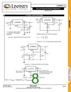
Even when the circuit is configured optimally, parasitic
resistance can be a significant source of error. A 100 mil. wide
PC trace built from 1 oz. copper-clad circuit board material has a
parasitic resistance of about 5 milliohms per inch of its length at
room temperature. If a 3-terminal regulator used to supply 2.50
volts is connected by 2 inches of this trace to a load which draws
5 amps of current, a 50 millivolt drop will appear between the
regulator and the load. Even when the regulator output voltage is
precisely 2.50 volts, the load will only see 2.45 volts, which is a
2% error. It is important to keep the connection between the
regulator output pin and the load as short as possible, and to use
wide traces or heavy-gauge wire.
Mcrosemi
2.8V
5.0A
50°C
IOUT
TA
R
2.7°C/W for TO-220
300 ft/min airflow available
.
Find:
Proper Heat Sink to keep IC’s junction temperature
below 125°C.**
Solution: The junction temperature is:
TJ = P (R + R + R ) + TA
D
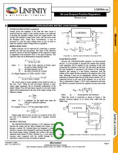
The minimum specified output capacitance for the regulator
should be located near the regulator package. If several capacitors
are used in parallel to construct the power system output
capacitance, any capacitors beyond the minimum needed to meet
the specified requirements of the regulator should be located near
the sections of the load that require rapidly-changing amounts of
current. Placing capacitors near the sources of load transients will
help ensure that power system transient response is not impaired
by the effects of trace impedance.
To maintain good load regulation, wide traces should be used
on the input side of the regulator, especially between the input
capacitors and the regulator. Input capacitor ESR must be small
enough that the voltage at the input pin does not drop below
VIN(MIN) during transients.
where: PD
Dissipated power.
R
Thermal resistance from the junction to
the mounting tab of the package.
Thermal resistance through the
interface between the IC and the
surface on which it is mounted.
(1.0°C/W at 6 in-lbs mounting screw
torque).
Thermal resistance from the mounting
surface to ambient (thermal resistance
of the heat sink).
T
R
R
TS
Heat Sink Temperature.
TJ
TC
TS
TA
V
= VOUT + VDROPOUT(MAX)
Rθ
Rθ
Rθ
SA
JT
CS
where: VIN(MIN)
the lowest allowable instantaneous
voltage at the input pin.
the designed output voltage for the
power supply system.
First, find the maximum allowable thermal resistance of the
heat sink:
VOUT
TJ − TA
R
=
−
(
R
+ R
)
SA
CS
VDROPOUT(MAX) the specified dropout voltage for the
installed regulator.
PD
=
−
= 5.0V −2.8V ×5.0A
( )
P
(V
IN(MAX)
VOUT )IOUT
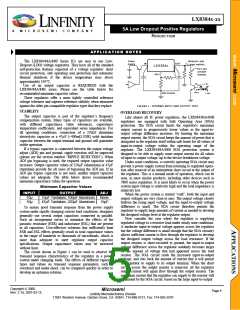
THERMAL CONSIDERATIONS
D
The LX8384/84A/84B regulators have internal power and
thermal limiting circuitry designed to protect each device under
overload conditions. For continuous normal load conditions,
however, maximum junction temperature ratings must not be
exceeded. It is important to give careful consideration to all
sources of thermal resistance from junction to ambient. This
includes junction to case, case to heat sink interface, and heat
sink thermal resistance itself.
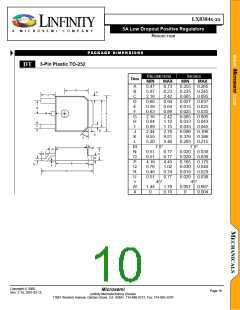
Junction-to-case thermal resistance is specified from the IC
junction to the back surface of the case directly opposite the die.
This is the lowest resistance path for heat flow. Proper mounting
is required to ensure the best possible thermal flow from this area
of the package to the heat sink. Thermal compound at the case to
heat sink interface is strongly recommended. If the case of the
device must be electrically isolated, a thermally conductive
spacer can be used, as long as its added contribution to thermal
resistance is considered. Note that the case of all devices in this
series is electrically connected to the output.
P =11.0W
D
125°C−50°C
(5.0V − 2.8V)*5.0A
= 3.1°C/W
R
=
−(2.7°C/W +1.0°C/W)
R
Next, select a suitable heat sink. The selected heat sink must
have R < 3.1°C/W. Thermalloy heatsink 6296B has R
3.0°C/W with 300ft/min air flow.
Finally, verify that junction temperature remains within speci-
fication using the selected heat sink:
=
=11W(2.7°C/W +1.0°C/W +3.0°C/W)+50°C
TJ
=124°C
TJ
** Although the device can operate up to 150°C junction, it is recommended for long
term reliability to keep the junction temperature below 125°C whenever possible.
Copyright 2000
Rev. 2.1d, 2001-03-15
Microsemi
Page 7
Linfinity Microelectronics Division
11861 Western Avenue, Garden Grove, CA. 92841, 714-898-8121, Fax: 714-893-2570

 MICROSEMI [ Microsemi ]