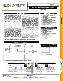
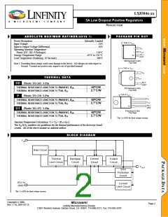
LX8384x-xx
ꢀꢁꢂꢃꢁꢂꢁꢄꢅꢆ
5A Low Dropout Positive Regulators
A
M I C R O S E M I
C O M P A N Y
PRODUCTION
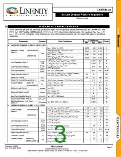
Unless otherwise specified, the following specifications apply over the operating ambient temperature for the LX8384x-xxC with
Mcrosemi
0°C ≤ TA ≤ 125°C and the LX8384-xxI with -25°C ≤ TA ≤ 125°C except where otherwise noted. Test conditions: VIN -VOUT = 3V;
IOUT = 5A. Low duty cycle pulse testing techniques are used which maintains junction and case temperatures equal to the ambient
temperature.
LX8384x-xx
Parameter
Symbol
Test Conditions
Units
Min
Typ
Max
.
LX8384-15 / 8384A-15 / 8384B-15 (1.5V FIXED)(CONTINUED)
ꢀ
Maximum Output Current
IOUT(MAX)
OUT(T)
VIN < 7V
5
6
A
%
%
Temperature Stability (Note 3)
Long Term Stability (Note 3)
0.25
0.3
OUT (t) TA=125°C, 1000 hours
1
RMS Output Noise (% of VOUT
(Note 3)
)
VOUT (RMS) TA=25°C, 10Hz < f < 10kHz
0.003
%
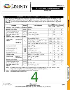
LX8384-33 / 8384A-33 / 8384B-33 (3.3V FIXED)
ꢀ
VIN=5V, IOUT=0mA, TA=25°C
4.75V < VIN < 10V, 0mA < IOUT < 5A, P < PMAX
VIN=5V, IOUT=0mA, TA=25°C
4.75V < VIN < 10V, 0mA < IOUT < 5A, P < PMAX
4.75V < VIN < 7V
3.267
3.235
3.274
3.267
3.30
3.30
3.30
3.30
1
3.333
3.365
3.326
3.333
6
V
V
Output Voltage
(Note 4)
LX8384/84A-33
LX8384B-33
VOUT
V
V
mV
mV
Line Regulation (Note 2)
OUT(VIN)
4.75V < VIN < 10V
2
10
OUT
Load Regulation (Note 2)
Thermal Regulation
VIN=5V, 0mA < IOUT < IOUT(MAX)
TA=25°C, 20ms pulse
5
15
mV
(IOUT
)
OUT
0.01
0.02
% / W
(Pwr)
Ripple Rejection (Note 3)
Quiescent Current
COUT=100µF (Tantalum), IOUT=5A
0mA < IOUT < IOUT(MAX), 4.75V < VIN < 10V
OUT=1%, IOUT < IOUT(MAX)
60
83
4
dB
mA
V
IQ
10
1.5
1.3
1.2
1
Dropout Voltage
LX8384-33
LX8384A/84B-33
OUT=1%, IOUT < IOUT(MAX)
V
Maximum Output Current
IOUT(MAX) VIN < 7V
OUT (T)
5
6
A
Temperature Stability (Note 3)
Long Term Stability (Note 3)
0.25
0.3
%
%
OUT (t) TA=125°C, 1000 hours
1
RMS Output Noise (% of VOUT
(Note 3)
)
VOUT (RMS) TA=25°C, 10Hz < f < 10kHz
0.003
%
Note 2
Regulation is measured at constant junction temperature, using pulse testing with a low duty cycle. Changes in output
voltage due to heating effects are covered under the specification for thermal regulation.
These parameters, although guaranteed are not tested in production.
Note 3
Note 4
See Maximum Output Current Section
Copyright 2000
Rev. 2.1d, 2001-03-15
Microsemi
Page 4
Linfinity Microelectronics Division
11861 Western Avenue, Garden Grove, CA. 92841, 714-898-8121, Fax: 714-893-2570

 MICROSEMI [ Microsemi ]