CCU 3000, CCU 3000-I
CCU 3001, CCU 3001-I
write:
bit 0 1... Write 8 bit
bit 1 1... Write 16 bit
bit 2 1... Read 8 bit
bit 3 1... Read 16 bit
done, thus deleting telegrams still waiting for access to
the bus. The IM bus addresses for the slave registers
are:
Slave register
IM bus address
02 H
fosc
1 byteData rate (5 bits) =
.
4
n
1
2
3
Only one of the bits 0 to 3 in the control register should
be set. If all bits are set to ‘0‘, a reset of the interface is
03 H
04 H
CPU
data bus
Slave
Interface
ID
Slave
1
Data
CLK
IM Bus addresses
2, 3 and 4
slave
Slave
2
register 1 (IM Bus
address 02H)
received data
(1 byte)
Slave
3
INT
INT
3
Contr.
Data
4
Mode
transmission
completed
Master
Ready
Master
Interface
Addr.
Rate
Data rate
n
fosc
fosc
.
f
IM
=
;
n =
Data rate:
.
4 n
f
4
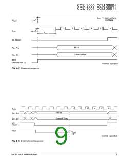
Fig. 2–13: IM bus interface
IM
MICRONAS INTERMETALL
13

 MICRONAS [ MICRONAS ]