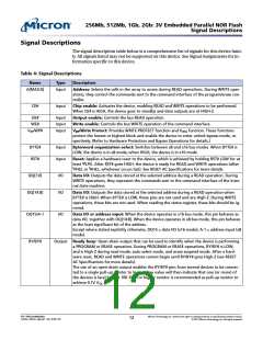
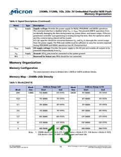
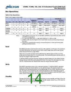
256Mb, 512Mb, 1Gb, 2Gb: 3V Embedded Parallel NOR Flash
Registers
Registers
Status Register
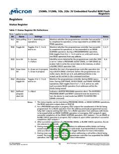
Table 7: Status Register Bit Definitions
Note 1 applies to entire table
Bit
Name
Settings
Description
Notes
DQ7 Data polling 0 or 1, depending on
Monitors whether the program/erase controller has successful- 2, 3, 4
ly completed its operation, or has responded to an ERASE SUS-
PEND operation.
bit
operations
DQ6 Toggle bit
Toggles: 0 to 1; 1 to 0;
and so on
Monitors whether the program/erase controller has successful- 3, 4, 5
ly completed its operations, or has responded to an ERASE
SUSPEND operation. During a PROGRAM/ERASE operation,
DQ6 toggles from 0 to 1, 1 to 0, and so on, with each succes-
sive READ operation from any address.
DQ5 Error bit
0 = Success
1 = Failure
Identifies errors detected by the program/erase controller. DQ5
is set to 1 when a PROGRAM, BLOCK ERASE, or CHIP ERASE op-
eration fails to write the correct data to the memory, or when
a BLANK CHECK operation fails.
4, 6
DQ3 Erase timer 0 = Erase not in progress Identifies the start of program/erase controller operation dur-
4
bit
1 = Erase in progress
ing a BLOCK ERASE command. Before the program/erase con-
troller starts, this bit set to 0, and additional blocks to be
erased can be written to the command interface.
DQ2 Alternative Toggles: 0 to 1; 1 to 0;
Monitors the program/erase controller during ERASE opera-
tions. During CHIP ERASE, BLOCK ERASE, and ERASE SUSPEND
operations, DQ2 toggles from 0 to 1, 1 to 0, and so on, with
each successive READ operation from addresses within the
blocks being erased.
3, 4
toggle bit
and so on
DQ1 Buffered
program
1 = Abort
Indicates a BUFFER PROGRAM operation abort. The BUFFERED
PROGRAM ABORT and RESET command must be issued to re-
turn the device to read mode (see WRITE TO BUFFER PRO-
GRAM command).
abort bit
1. The status register can be read during PROGRAM, ERASE, or ERASE SUSPEND operations;
the READ operation outputs data on DQ[7:0].
Notes:
2. For a PROGRAM operation in progress, DQ7 outputs the complement of the bit being
programmed. For a READ operation from the address previously programmed success-
fully, DQ7 outputs existing DQ7 data. For a READ operation from addresses with blocks
to be erased while an ERASE SUSPEND operation is in progress, DQ7 outputs 0; upon
successful completion of the ERASE SUSPEND operation, DQ7 outputs 1. For an ERASE or
BLANK CHECK operation in progress, DQ7 outputs 0; upon either operation's successful
completion, DQ7 outputs 1.
3. After successful completion of a PROGRAM, ERASE, or BLANK CHECK operation, the de-
vice returns to read mode.
4. During erase suspend mode, READ operations to addresses within blocks not being
erased output memory array data as if in read mode. A protected block is treated the
same as a block not being erased. See the Toggle Flowchart for more information.
5. During erase suspend mode, DQ6 toggles when addressing a cell within a block being
erased. The toggling stops when the program/erase controller has suspended the ERASE
operation. See the Toggle Flowchart for more information.
PDF: 09005aef849b4b09
m29ew_256mb_2gb.pdf - Rev. B 8/12 EN
Micron Technology, Inc. reserves the right to change products or specifications without notice.
16
© 2012 Micron Technology, Inc. All rights reserved.

 MICRON [ MICRON TECHNOLOGY ]