TC7109/A
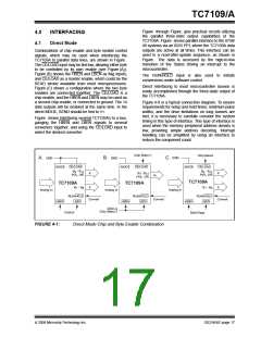
Conversions may be obtained on command under soft-
ware control by driving the RUN/HOLD input to the
TC7109A by a bit of the 8255. Another peripheral
device may be serviced by the unused port of the 8255.
4.2
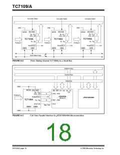
Handshake Mode
The Handshake mode provides an interface to a wide
variety of external devices. The byte enables may be
used as byte identification flags, or as load enables,
and external latches may be clocked by the rising edge
of CE/LOAD. A handshake interface to Intel® micropro-
cessors using an 8255 PPI is shown in Figure . The
handshake operation with the 8255 is controlled by
inverting its Input Buffer Full (IBF) flag to drive the
SEND input to the TC7109A, and using the CE/LOAD
to drive the 8255 strobe. The internal control register of
the PPI should be set in MODE 1 for the port used. If
the 8255 IBF flag is LOW and the TC7109A is in Hand-
shake mode, the next word will be strobed into the port.
The strobe will cause IBF to go HIGH (SEND goes
LOW), which will keep the enabled byte outputs active.
The PPI will generate an interrupt which, when
executed, will result in the data being read. The IBF will
be reset LOW when the byte is read, causing the
TC7109A to sequence into the next byte. The MODE
input to the TC7109A is connected to the control line on
the PPI.
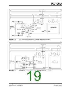
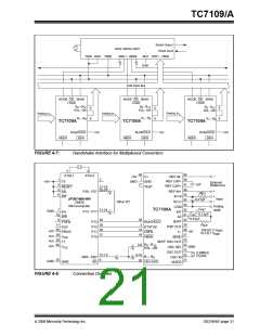
The Handshake mode is particularly useful for directly
interfacing to industry standard UARTs (such as Intersil
HD-6402), providing a means of serially transmitting
converted data with minimum component count.
A typical UART connection is shown in Figure . In this
circuit, any word received by the UART causes the
UART DR (Data Ready) output to go HIGH. The MODE
input to the TC7109A goes HIGH, triggering the
TC7109A into Handshake mode. The high order byte is
output to the UART and when the UART has trans-
ferred the data to the Transmitter register, TBRE
(SEND) goes HIGH again, LBEN will go HIGH, driving
the UART DRR (Data Ready Reset), which will signal
the end of the transfer of data from the TC7109A to the
UART.
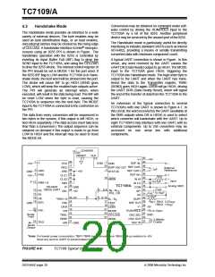
An extension of the typical connection to several
TC7109A’s with one UART is shown in Figure 4-7. In
this circuit, the word received by the UART (available at
the RBR outputs when DR is HIGH) is used to select
which converter will handshake with the UART. Up to
eight TC7109A’s may interface with one UART, with no
external components. Up to 256 converters may be
accessed on one serial line with additional
components.
The data from every conversion will be sequenced in
two bytes in the system, if this output is left HIGH, or
tied HIGH separately. (The data access must take less
time than a conversion.) The output sequence can be
obtained on demand if this output is made to go from
LOW to HIGH and the interrupt may be used to reset
the MODE bit.
CD4060B
15
Q3
RESET
11
CLK
10
40
+5V
V+
REF IN-
1
40
17
39
38
37
36
35
34
1
25
2
39
38
37
36
35
34
33
32
31
30
29
28
26
24
23
22
V
GND
–
+5V
TRC
RRC
EPE
CLS1
CLS2
SBS
PI
GND
REF CAP-
REF CAP+
REF IN+
BUFF OSC OUT
STATUS
External
Reference
1μF
1MΩ
3
4
GND
RRD
+5V
GND
+5V
+
19
+
IN HI
HBEN
Input
–
Analog GND
0.01μF
5–12
RBR1–8
IN LO
TC7109A
HD-640R
CMOS UART
GND
+5V
COM
INT
C
6
8
13
14
15
16
3–8
INT
B
- B ,
12
POL, OR
PE
9
CRL
C
0.15μF
AZ
FE
AZ
0.33μF
8
26–33
24
9–16
17
OE
SFD
BUFF
*TBR1–8
TRE
B - B
1
8
R
20kΩ 0.2V
REF
INT
REF OUT
V-
GND
TEST
100kΩ 1V
REF
18
18
-5V
DRR
DR
LBEN
20
19
21
RR1
TRO
RUN/HOLD
+5V or Open
GND
MODE
CE/LOAD
SEND
23
20
Serial
Input
OSC SEL
OSC OUT
OSC IN
TBRL
TBRE
MR
22
27
3.58MHz
Crystal
21
25
Serial
Output
GND
*Note: For lowest power consumption, TBR1-TBR8 inputs should have 100kΩ pull-up resistors to +5V.
Send any word to UART to transmit latest result.
FIGURE 4-6:
TC7109 Typical UART Interface
DS21456C-page 20
© 2006 Microchip Technology Inc.

 MICROCHIP [ MICROCHIP ]