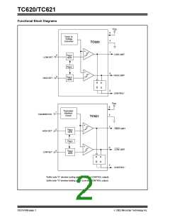
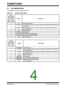
TC620/TC621
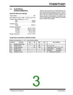
1.0
ELECTRICAL
CHARACTERISTICS
*Stresses above those listed under "Absolute Maximum Rat-
ings" may cause permanent damage to the device. These are
stress ratings only and functional operation of the device at
these or any other conditions above those indicated in the
operation sections of the specifications is not implied. Expo-
sure to Absolute Maximum Rating conditions for extended
periods may affect device reliability.
Absolute Maximum Ratings*
Supply Voltage ....................................................... 20V
Input Voltage Any Input.. (GND – 0.3V) to (V +0.3V)
DD
Package Power Dissipation (T ≤ 70°C)
A
PDIP ..............................................730mW
SOIC ..............................................470mW
Derating Factors:
Plastic ........................................... 8mW/°C
Operating Temperature:
M Version......................... -55°C to +125°C
V Version ......................... -40°C to +125°C
E Version ........................... -40°C to +85°C
C Version .............................. 0°C to +70°C
Storage Temperature ......................... -65°C to +150°C
TC620/TC621 ELECTRICAL SPECIFICATIONS
Electrical Characteristics: TA = 25°C, unless otherwise specified.
Symbol
Parameter
Min
Typ
Max
Unit
Test Conditions
VDD
IDD
Supply Voltage Range
Supply Current
4.5
—
—
270
400
—
18
400
1000
1
V
µA
W
5V ≤ VDD ≤ 18V
Output High or Low, 5V ≤ VDD ≤ 18V
ROUT
IOUT
IOUT
TERR
Output Resistance
Output Current
—
—
mA
mA
°C
Temp Sensed
Cool/Heat
Source/Sink
Source/Sink
Output Current
—
—
1
Absolute Accuracy
T - 3
T
T + 3
T = Programmed Temperature
2002 Microchip Technology Inc.
DS21439B-page 3

 MICROCHIP [ MICROCHIP ]