Super I/O with Temperature Sensing, Quiet Auto Fan and Glue Logic
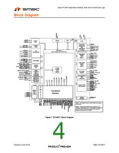
Block Diagram
WDT*
CLK32
WDT
Speaker
CLOCK
GEN
LEDs
CLOCKI
PD[7,0]
Multi-Mode
Parallel Port
with
SER_IRQ
PCI_CLK
SERIAL
IRQ
BUSY, SLCT, PE,
nERROR, nACK
ChiProtectTM
FDC MUX
/
nSTROBE, nINIT,
nSLCTIN, nALF
LAD[3:0]
LFrame#
Internal Bus
(Data, Address, and Control lines)
LPC
Bus Interface
(see LPC47B27x)
TXD1*, RXD1
High-Speed
16550A
UART
LDRQ#
nCTS1, nRTS1*
PCI_RESET#
nDSR1, nDTR1
nDCD1, nRI1
PORT 1
IO_PME_S3*
IO_PME_S5*
IO_SMI*
Power Mgmt
TXD2 (IRTX)*,
RXD2 (IRRX)*
High-Speed
16550A
UART
GP1[0:4]*, GP21*,GP22*
CTS2*, RTS2 *
DSR2*, DTR2*
DCD2*, RI2*
GP27*, GP32*,GP33*
GP36*, GP37* , GP4[0,2,3]*
GP5[0:1]*, GP6[0:1]*
General
Purpose
I/O
PORT 2
32 byte
Security
Key
SMSC
Proprietary
82077
nMTR0, nTRK0, InNDEX
nWGATE, nHDSEL
nIDE_RSTDRV*
PCI Reset
Outputs
Register
nPCIRST_OUT[1:4]*
DRVDEN0*, nWRTPRT
nDIR, nSTEP
Compatible
Floppydisk
Controller with
Digital Data
Separator &
Write Precom-
pensation
MCLK*, MDAT*
A20M*
nKBDRST*
Keyboard/Mouse
8042
controller
nDSKCHG, nDS0,
KCLK*, KDAT*
nRDATA, nWDATA
nFPRST, PB_IN#
PWRGD_PS
SLP_S3#, SLP_S5#
`
PWRGD_CPU ,
PWRGD_3V
n3VSB_GAT E
n3V_GATE
Power Control
and Recovery
S
M
b
nRSMRST
SMbus
Isola-
tion
Hardware
Monitor
SDA1
SCLK1
SDA2
Switch
u
SCLK2
Intruder
Detection
s
nINTRD_IN
Note 1: This diagram does not show power and ground
connections.
Note 2: Signal names followed by an asterisk (*) are
located on multifunction pins. This diagram is designed to
show the various functions available on the chip and
should not be used as a pin layout.
Figure 1 SCH5017 Block Diagram
Revision 0.5 (05-24-07)
4
SMSC SCH5017
PRODUCT PREVIEW

 MICROCHIP [ MICROCHIP ]