PIC18F2480/2580/4480/4580
The inclusion of an internal RC oscillator also provides
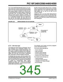
the additional benefits of a Fail-Safe Clock Monitor
(FSCM) and Two-Speed Start-up. FSCM provides for
25.0 SPECIAL FEATURES OF
THE CPU
background monitoring of the peripheral clock and
automatic switchover in the event of its failure. Two-
Speed Start-up enables code to be executed almost
immediately on start-up, while the primary clock source
completes its start-up delays.
PIC18F2480/2580/4480/4580 devices include several
features intended to maximize reliability and minimize
cost through elimination of external components.
These are:
• Oscillator Selection
• Resets:
All of these features are enabled and configured by
setting the appropriate Configuration register bits.
- Power-on Reset (POR)
- Power-up Timer (PWRT)
- Oscillator Start-up Timer (OST)
- Brown-out Reset (BOR)
• Interrupts
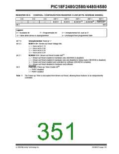
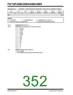
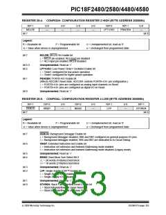
25.1 Configuration Bits
The Configuration bits can be programmed (read as
‘0’) or left unprogrammed (read as ‘1’) to select various
device configurations. These bits are mapped starting
at program memory location 300000h.
• Watchdog Timer (WDT)
• Fail-Safe Clock Monitor
• Two-Speed Start-up
• Code Protection
The user will note that address 300000h is beyond the
user program memory space. In fact, it belongs to the
configuration memory space (300000h-3FFFFFh), which
can only be accessed using table reads and table writes.
• ID Locations
• In-Circuit Serial Programming
Programming the Configuration registers is done in a
manner similar to programming the Flash memory. The
WR bit in the EECON1 register starts a self-timed write
to the Configuration register. In normal operation
mode, a TBLWTinstruction with the TBLPTR pointing to
the Configuration register sets up the address and the
data for the Configuration register write. Setting the WR
bit starts a long write to the Configuration register. The
Configuration registers are written a byte at a time. To
write or erase a configuration cell, a TBLWTinstruction
can write a ‘1’ or a ‘0’ into the cell. For additional details
on Flash programming, refer to Section 7.5 “Writing
to Flash Program Memory”.
The oscillator can be configured for the application
depending on frequency, power, accuracy and cost. All
of the options are discussed in detail in Section 3.0
“Oscillator Configurations”.
A complete discussion of device Resets and interrupts
is available in previous sections of this data sheet.
In addition to their Power-up and Oscillator Start-up
Timers provided for Resets, PIC18F2480/2580/4480/
4580 devices have a Watchdog Timer, which is either
permanently enabled via the Configuration bits or
software controlled (if configured as disabled).
TABLE 25-1: CONFIGURATION BITS AND DEVICE IDs
Default/
Unprogrammed
Value
File Name
Bit 7
Bit 6
Bit 5
Bit 4
Bit 3
Bit 2
Bit 1
Bit 0
300001h CONFIG1H
300002h CONFIG2L
300003h CONFIG2H
IESO
—
FCMEN
—
—
—
FOSC3
FOSC2
FOSC1
FOSC0
00-- 0111
---1 1111
---1 1111
1--- -01-
10-0 -1-1
---- 1111
11-- ----
---- 1111
111- ----
---- 1111
-1-- ----
—
—
—
BORV1
BORV0 BOREN1 BOREN0 PWRTEN
—
—
WDTPS3 WDTPS2 WDTPS1 WDTPS0 WDTEN
300005h CONFIG3H MCLRE
—
—
BBSIZ
—
—
—
LPT1OSC PBADEN
—
STVREN
CP0
300006h CONFIG4L DEBUG XINST
—
LVP
CP2
—
—
CP1
—
300008h CONFIG5L
300009h CONFIG5H
30000Ah CONFIG6L
—
CPD
—
—
CPB
—
—
CP3
—
—
—
—
—
—
WRT3
—
WRT2
—
WRT1
—
WRT0
—
30000Bh CONFIG6H WRTD
WRTB
—
WRTC
—
—
30000Ch CONFIG7L
30000Dh CONFIG7H
3FFFFEh DEVID1
3FFFFFh DEVID2
—
—
—
EBTR3
—
EBTR2
—
EBTR1
—
EBTR0
—
EBTRB
DEV1
DEV9
—
—
(1)
DEV2
DEV10
DEV0
DEV8
REV4
DEV7
REV3
DEV6
REV2
DEV5
REV1
DEV4
REV0
DEV3
xxxx xxxx
0000 1100
Legend:
x= unknown, u= unchanged, - = unimplemented, q= value depends on condition.
Shaded cells are unimplemented, read as ‘0’.
Note 1: See Register 25-12 for DEVID1 values. DEVID registers are read-only and cannot be programmed by the user.
© 2009 Microchip Technology Inc.
DS39637D-page 349

 MICROCHIP [ MICROCHIP ]