PIC18F2480/2580/4480/4580
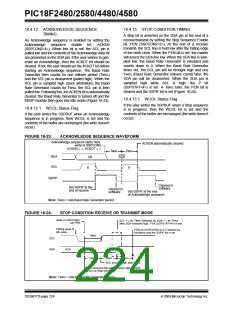
18.4.12 ACKNOWLEDGE SEQUENCE
TIMING
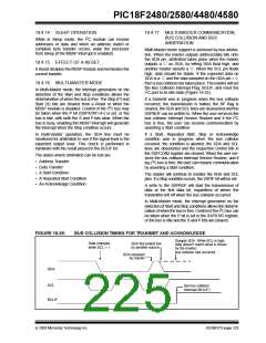
18.4.13 STOP CONDITION TIMING
A Stop bit is asserted on the SDA pin at the end of a
receive/transmit by setting the Stop Sequence Enable
bit, PEN (SSPCON2<2>). At the end of a receive/
transmit, the SCL line is held low after the falling edge
of the ninth clock. When the PEN bit is set, the master
will assert the SDA line low. When the SDA line is sam-
pled low, the Baud Rate Generator is reloaded and
counts down to 0. When the Baud Rate Generator
times out, the SCL pin will be brought high and one
TBRG (Baud Rate Generator rollover count) later, the
SDA pin will be deasserted. When the SDA pin is
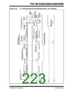
An Acknowledge sequence is enabled by setting the
Acknowledge
sequence
enable
bit,
ACKEN
(SSPCON2<4>). When this bit is set, the SCL pin is
pulled low and the contents of the Acknowledge data bit
are presented on the SDA pin. If the user wishes to gen-
erate an Acknowledge, then the ACKDT bit should be
cleared. If not, the user should set the ACKDT bit before
starting an Acknowledge sequence. The Baud Rate
Generator then counts for one rollover period (TBRG)
and the SCL pin is deasserted (pulled high). When the
SCL pin is sampled high (clock arbitration), the Baud
Rate Generator counts for TBRG; the SCL pin is then
pulled low. Following this, the ACKEN bit is automatically
cleared, the Baud Rate Generator is turned off and the
MSSP module then goes into Idle mode (Figure 18-23).
sampled high while SCL is high, the
(SSPSTAT<4>) is set. A TBRG later, the PEN bit is
cleared and the SSPIF bit is set (Figure 18-24).
P
bit
18.4.13.1 WCOL Status Flag
If the user writes the SSPBUF when a Stop sequence
is in progress, then the WCOL bit is set and the
contents of the buffer are unchanged (the write doesn’t
occur).
18.4.12.1 WCOL Status Flag
If the user writes the SSPBUF when an Acknowledge
sequence is in progress, then WCOL is set and the
contents of the buffer are unchanged (the write doesn’t
occur).
FIGURE 18-23:
ACKNOWLEDGE SEQUENCE WAVEFORM
Acknowledge sequence starts here,
write to SSPCON2
ACKEN automatically cleared
ACKEN = 1, ACKDT = 0
TBRG
TBRG
SDA
D0
ACK
SCL
8
9
SSPIF
Cleared in
software
Set SSPIF at the
end of receive
Cleared in
software
Set SSPIF at the end
of Acknowledge sequence
Note: TBRG = one Baud Rate Generator period.
FIGURE 18-24:
STOP CONDITION RECEIVE OR TRANSMIT MODE
Write to SSPCON2,
set PEN
SCL = 1for TBRG, followed by SDA = 1for TBRG
after SDA sampled high, P bit (SSPSTAT<4>) is set
Falling edge of
9th clock
PEN bit (SSPCON2<2>) is cleared by
hardware and the SSPIF bit is set
TBRG
SCL
ACK
SDA
P
TBRG
TBRG
TBRG
SCL brought high after TBRG
SDA asserted low before rising edge of clock
to set up Stop condition
Note: TBRG = one Baud Rate Generator period.
DS39637D-page 224
© 2009 Microchip Technology Inc.

 MICROCHIP [ MICROCHIP ]