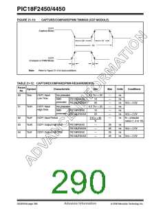
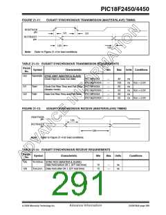
PIC18F2450/4450
TABLE 21-18: A/D CONVERSION REQUIREMENTS
Param
Symbol
Characteristic
Min
Max
Units
Conditions
No.
130
TAD
A/D Clock Period
PIC18FXXXX
0.7
1.4
25.0(1)
25.0(1)
μs TOSC based, VREF ≥ 3.0V
PIC18LFXXXX
μs VDD = 2.0V,
TOSC based, VREF full range
PIC18FXXXX
TBD
TBD
1
3
μs A/D RC mode
PIC18LFXXXX
μs VDD = 2.0V,
A/D RC mode
131
132
TCNV
TACQ
Conversion Time
11
12
TAD
(not including acquisition time)(2)
Acquisition Time(3)
1.4
TBD
—
—
μs -40°C to +85°C
μs
0°C ≤ to ≤ +85°C
135
137
TSWC
TDIS
Switching Time from Convert → Sample
Discharge Time
—
(Note 4)
0.2
—
μs
Legend: TBD = To Be Determined
Note 1: The time of the A/D clock period is dependent on the device frequency and the TAD clock divider.
2: ADRES registers may be read on the following TCY cycle.
3: The time for the holding capacitor to acquire the “New” input voltage when the voltage changes full scale
after the conversion (VDD to VSS or VSS to VDD). The source impedance (RS) on the input channels is 50Ω.
4: On the following cycle of the device clock.
DS39760A-page 292
Advance Information
© 2006 Microchip Technology Inc.

 MICROCHIP [ MICROCHIP ]