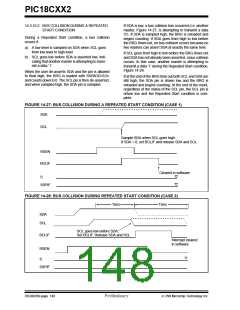
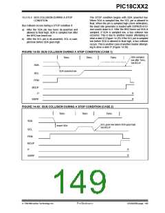
PIC18CXX2
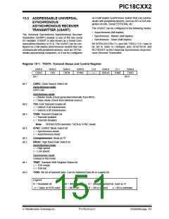
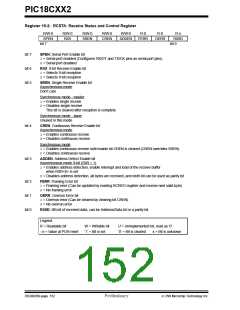
Register 15-2: RCSTA: Receive Status and Control Register
R/W-0
SPEN
R/W-0
RX9
R/W-0
SREN
R/W-0
CREN
R/W-0
R-0
R-0
R-x
ADDEN
FERR
OERR
RX9D
bit 7
bit 0
bit 7
bit 6
bit 5
SPEN: Serial Port Enable bit
1= Serial port enabled (Configures RX/DT and TX/CK pins as serial port pins)
0= Serial port disabled
RX9: 9-bit Receive Enable bit
1= Selects 9-bit reception
0= Selects 8-bit reception
SREN: Single Receive Enable bit
Asynchronous mode
Don’t care
Synchronous mode - master
1= Enables single receive
0= Disables single receive
This bit is cleared after reception is complete.
Synchronous mode - slave
Unused in this mode
bit 4
CREN: Continuous Receive Enable bit
Asynchronous mode
1= Enables continuous receive
0= Disables continuous receive
Synchronous mode
1= Enables continuous receive until enable bit CREN is cleared (CREN overrides SREN)
0= Disables continuous receive
bit 3
ADDEN: Address Detect Enable bit
Asynchronous mode 9-bit (RX9 = 1)
1= Enables address detection, enable interrupt and load of the receive buffer
when RSR<8> is set
0= Disables address detection, all bytes are received, and ninth bit can be used as parity bit
bit 2
bit 1
bit 0
FERR: Framing Error bit
1= Framing error (Can be updated by reading RCREG register and receive next valid byte)
0= No framing error
OERR: Overrun Error bit
1= Overrun error (Can be cleared by clearing bit CREN)
0= No overrun error
RX9D: 9th bit of received data, can be Address/Data bit or a parity bit.
Legend:
R = Readable bit
W = Writable bit
’1’ = Bit is set
U = Unimplemented bit, read as ‘0’
’0’ = Bit is cleared x = Bit is unknown
- n = Value at POR reset
DS39026B-page 152
Preliminary
7/99 Microchip Technology Inc.

 MICROCHIP [ MICROCHIP ]