PIC17C4X
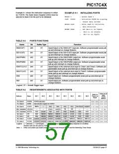
Example 9-1 shows the instruction sequence to initial-
ize PORTB. The Bank Select Register (BSR) must be
selected to Bank 0 for the port to be initialized.
EXAMPLE 9-1: INITIALIZING PORTB
MOVLB 0
; Select Bank 0
; Initialize PORTB by clearing
output data latches
; Value used to initialize
CLRF PORTB
;
MOVLW 0xCF
MOVWF DDRB
;
;
;
;
data direction
Set RB<3:0> as inputs
RB<5:4> as outputs
RB<7:6> as inputs
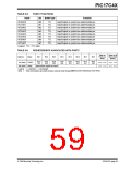
TABLE 9-3:
PORTB FUNCTIONS
Name
Bit
Buffer Type
Function
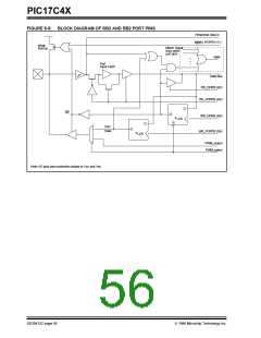
RB0/CAP1
bit0
ST
Input/Output or the RB0/CAP1 input pin. Software programmable weak pull-
up and interrupt on change features.
RB1/CAP2
RB2/PWM1
RB3/PWM2
RB4/TCLK12
RB5/TCLK3
RB6
bit1
bit2
bit3
bit4
bit5
bit6
bit7
ST
ST
ST
ST
ST
ST
ST
Input/Output or the RB1/CAP2 input pin. Software programmable weak pull-
up and interrupt on change features.
Input/Output or the RB2/PWM1 output pin. Software programmable weak
pull-up and interrupt on change features.
Input/Output or the RB3/PWM2 output pin. Software programmable weak
pull-up and interrupt on change features.
Input/Output or the external clock input to Timer1 and Timer2. Software pro-
grammable weak pull-up and interrupt on change features.
Input/Output or the external clock input to Timer3. Software programmable
weak pull-up and interrupt on change features.
Input/Output pin. Software programmable weak pull-up and interrupt on
change features.
RB7
Input/Output pin. Software programmable weak pull-up and interrupt on
change features.
Legend: ST = Schmitt Trigger input.
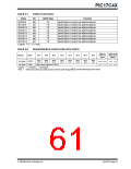
TABLE 9-4:
REGISTERS/BITS ASSOCIATED WITH PORTB
Value on all
Value on
other
resets
(Note1)
Address
Name
Bit 7
Bit 6
Bit 5
Bit 4
Bit 3
Bit 2
Bit 1
Bit 0
Power-on
Reset
12h, Bank 0
11h, Bank 0
PORTB
DDRB
PORTB data latch
Data direction register for PORTB
xxxx xxxx uuuu uuuu
1111 1111 1111 1111
10h, Bank 0
PORTA
RBPU
—
RA5
RA4
RA3
RA2
RA1/T0CKI RA0/INT 0-xx xxxx 0-uu uuuu
06h, Unbanked CPUSTA
07h, Unbanked INTSTA
—
—
STKAV
T0IF
GLINTD
INTF
TO
PD
—
—
--11 11-- --11 qq--
0000 0000 0000 0000
0000 0010 0000 0010
0000 0000 0000 0000
PEIF
RBIF
RBIE
T0CKIF
TMR3IF
TMR3IE
PEIE
CA2IF
CA2IE
T16
T0CKIE
CA1IF
CA1IE
T0IE
TXIF
TXIE
INTE
RCIF
RCIE
16h, Bank 1
17h, Bank 1
16h, Bank 3
PIR
TMR2IF
TMR2IE
TMR1IF
TMR1IE
CA1ED0
PIE
TCON1
CA2ED1 CA2ED0 CA1ED1
TMR3CS TMR2CS TMR1CS 0000 0000 0000 0000
17h, Bank 3
TCON2
CA2OVF CA1OVF PWM2ON PWM1ON CA1/PR3 TMR3ON TMR2ON TMR1ON 0000 0000 0000 0000
Legend: x= unknown, u= unchanged, - = unimplemented read as '0', q = Value depends on condition.
Shaded cells are not used by PORTB.
Note 1: Other (non power-up) resets include: external reset through MCLR and the Watchdog Timer Reset.
1996 Microchip Technology Inc.
DS30412C-page 57

 MICROCHIP [ MICROCHIP ]