PIC17C4X
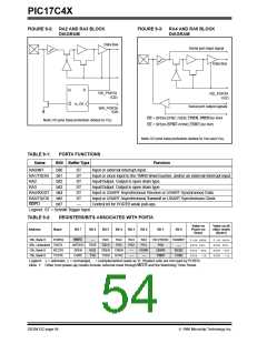
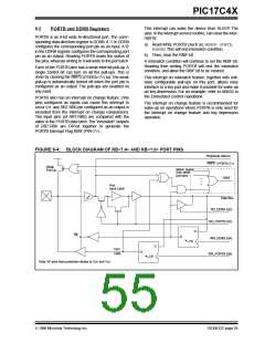
FIGURE 9-2: RA2 AND RA3 BLOCK
DIAGRAM
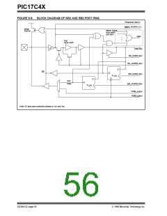
FIGURE 9-3: RA4 AND RA5 BLOCK
DIAGRAM
Data Bus
Serial port input signal
Data Bus
Q
Q
D
RD_PORTA
(Q2)
RD_PORTA
(Q2)
CK
Serial port output signals
WR_PORTA
(Q4)
OE = SPEN,SYNC,TXEN, CREN, SREN for RA4
OE = SPEN (SYNC+SYNC,CSRC) for RA5
Note: I/O pins have protection diodes to VSS.
Note: I/O pins have protection diodes to VDD and VSS.
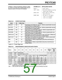
TABLE 9-1:
PORTA FUNCTIONS
Bit0 Buffer Type
Name
Function
RA0/INT
RA1/T0CKI
RA2
bit0
bit1
bit2
bit3
bit4
bit5
bit7
ST
ST
ST
ST
ST
ST
—
Input or external interrupt input.
Input or clock input to the TMR0 timer/counter, and/or an external interrupt input.
Input/Output. Output is open drain type.
RA3
Input/Output. Output is open drain type.
RA4/RX/DT
RA5/TX/CK
RBPU
Input or USART Asynchronous Receive or USART Synchronous Data.
Input or USART Asynchronous Transmit or USART Synchronous Clock.
Control bit for PORTB weak pull-ups.
Legend: ST = Schmitt Trigger input.
TABLE 9-2:
REGISTERS/BITS ASSOCIATED WITH PORTA
Value on
Power-on
Reset
Value on all
other resets
(Note1)
Address
Name
Bit 7
Bit 6
Bit 5
Bit 4
Bit 3
Bit 2
Bit 1
Bit 0
10h, Bank 0
PORTA
RBPU
INTEDG
SPEN
—
RA5
T0CS
SREN
TXEN
RA4
PS3
RA3
PS2
—
RA2
PS1
FERR
—
RA1/T0CKI RA0/INT
0-xx xxxx
0000 000-
0000 -00x
0000 --1x
0-uu uuuu
0000 000-
0000 -00u
0000 --1u
05h, Unbanked T0STA
T0SE
RC9
TX9
PS0
—
13h, Bank 0
15h, Bank 0
RCSTA
TXSTA
CREN
SYNC
OERR
TRMT
RC9D
TX9D
CSRC
—
Legend: x= unknown, u= unchanged, -= unimplemented reads as '0'. Shaded cells are not used by PORTA.
Note 1: Other (non power-up) resets include: external reset through MCLR and the Watchdog Timer Reset.
DS30412C-page 54
1996 Microchip Technology Inc.

 MICROCHIP [ MICROCHIP ]