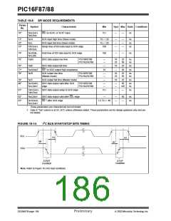
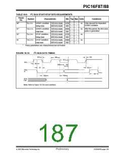
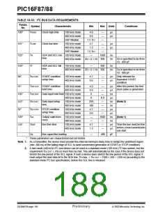
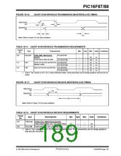
PIC16F87/88
TABLE 18-13: A/D CONVERTER CHARACTERISTICS: PIC16F87/88 (INDUSTRIAL, EXTENDED)
PIC16LF87/88 (INDUSTRIAL)
Param
No.
Sym
NR
Characteristic
Resolution
Min
—
Typ†
—
Max
10 bits
< ± 1
< ± 1
< ± 2
< ± 1
Units
Conditions
A01
bit VREF = VDD = 5.12V,
VSS ≤ VAIN ≤ VREF
A03
A04
A06
A07
EIL
Integral linearity error
—
—
LSb VREF = VDD = 5.12V,
VSS ≤ VAIN ≤ VREF
EDL
Differential linearity error
—
—
LSb VREF = VDD = 5.12V,
VSS ≤ VAIN ≤ VREF
EOFF Offset error
—
—
LSb VREF = VDD = 5.12V,
VSS ≤ VAIN ≤ VREF
EGN
Gain error
—
—
LSb VREF = VDD = 5.12V,
VSS ≤ VAIN ≤ VREF
(3)
A10
A20
—
Monotonicity
—
guaranteed
—
—
VSS ≤ VAIN ≤ VREF
VREF Reference Voltage
2.5
2.2
—
—
VDD + 0.3
VDD + 0.3
V
V
-40°C to +85°C
0°C to +85°C
A21
A22
A25
A30
VREF+ Reference voltage high
VREF- Reference voltage low
AVDD – 2.5V
AVSS – 0.3V
VSS – 0.3V
—
AVDD + 0.3V
VREF+ – 2.0V
VREF + 0.3V
2.5
V
V
V
VAIN
ZAIN
Analog input voltage
—
—
Recommended impedance of
analog voltage source
kΩ See (Note 4)
(2)
A50
IREF
VREF input current
—
—
5
µA During VAIN acquisition.
Based on differential of VHOLD to
VAIN to charge CHOLD, see
Section 12.1 “A/D Acquisition
Requirements”.
—
—
500
µA During A/D Conversion cycle.
†
Data in “Typ” column is at 5V, 25°C unless otherwise stated. These parameters are for design guidance only and are not
tested.
Note 1: VREF current is from RA3 pin or VDD pin, whichever is selected as reference input.
2: The A/D conversion result never decreases with an increase in the input voltage, and has no missing codes.
3: The maximum allowed impedance for analog voltage source is 10 kΩ. This requires higher acquisition times.
DS30487B-page 188
Preliminary
2003 Microchip Technology Inc.

 MICROCHIP [ MICROCHIP ]