PIC16F87/88
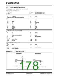
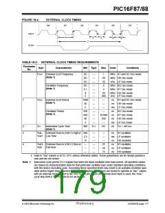
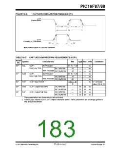
FIGURE 18-4:
EXTERNAL CLOCK TIMING
Q4
Q1
Q2
Q3
Q4
Q1
OSC1
CLKO
1
3
4
4
3
2
TABLE 18-3: EXTERNAL CLOCK TIMING REQUIREMENTS
Parameter
Sym
Characteristic
Min Typ†
Max
Units
Conditions
No.
FOSC External CLKI Frequency
DC
DC
DC
DC
0.1
—
—
—
—
—
1
20
32
4
MHz XT and RC Osc mode
MHz HS Osc mode
kHz LP Osc mode
(Note 1)
Oscillator Frequency
(Note 1)
MHz RC Osc mode
MHz XT Osc mode
4
4
5
—
—
20
200
MHz HS Osc mode
kHz LP Osc mode
1
TOSC
External CLKI Period
(Note 1)
1000
50
—
—
—
—
ns XT and RC Osc mode
ns HS Osc mode
ms LP Osc mode
ns RC Osc mode
ns XT Osc mode
ns HS Osc mode
ms LP Osc mode
ns TCY = 4/FOSC
5
—
—
Oscillator Period
(Note 1)
250
250
50
—
—
—
10,000
250
—
—
5
—
2
3
TCY
Instruction Cycle Time
(Note 1)
200
TCY
DC
TosL, External Clock in (OSC1) High or 500
TosH Low Time
—
—
—
—
—
—
—
—
—
25
50
15
ns XT oscillator
ms LP oscillator
ns HS oscillator
ns XT oscillator
ns LP oscillator
ns HS oscillator
2.5
15
4
TosR, External Clock in (OSC1) Rise or
TosF Fall Time
—
—
—
†
Data in “Typ” column is at 5V, 25°C unless otherwise stated. These parameters are for design guidance
only and are not tested.
Note 1: Instruction cycle period (TCY) equals four times the input oscillator time base period. All specified values
are based on characterization data for that particular oscillator type under standard operating conditions,
with the device executing code. Exceeding these specified limits may result in an unstable oscillator oper-
ation and/or higher than expected current consumption. All devices are tested to operate at “min.” values
with an external clock applied to the OSC1/CLKI pin. When an external clock input is used, the “max.”
cycle time limit is “DC” (no clock) for all devices.
2003 Microchip Technology Inc.
Preliminary
DS30487B-page 177

 MICROCHIP [ MICROCHIP ]