PIC16F5X
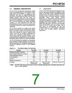
FIGURE 2-1:
PIC16F5X SERIES BLOCK DIAGRAM
9-11
Flash
512 X 12 (F54)
2048 X 12(F57)
2048 x 12(F59)
T0CKI
Pin
OSC1 OSC2 MCLR
Configuration Word
“Disable”
9-11
Stack 1
Stack 2
“Osc
Select”
PC
Watchdog
Timer
12
2
“Code-
Oscillator/
Timing &
Control
Protect”
Instruction
Register
CLKOUT
WDT/TMR0
Prescaler
9
WDT
Time-out
12
8
“Sleep”
Instruction
Decoder
6
“Option”
Option Reg.
From W
Direct Address
Direct RAM
Address
General
Purpose
Register
File
(SRAM)
25, 72 or 134
Bytes
5
5-7
8
STATUS
ALU
TMR0
SFR
8
Data Bus
W
8
From W
8
From W
4
From W
8
8
8
4
TRISB PORTB
TRISA PORTA
TRISC
PORTC
8
4
8
“TRIS 7”
“TRIS 6”
“TRIS 5”
RC<7:0>
RA<3:0>
RB<7:0>
PIC16F57/59
only
From W
From W
4
8
8
8
TRISD
PORTD
8
TRISE
PORTE
4
“TRIS 8”
RD<7:0>
“TRIS 9”
RE<7:4>
PIC16F59
only
PIC16F59
only
DS41213D-page 8
© 2007 Microchip Technology Inc.

 MICROCHIP [ MICROCHIP ]