PIC16F7X7
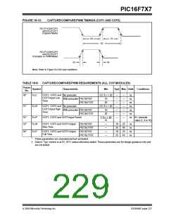
FIGURE 18-10:
CAPTURE/COMPARE/PWM TIMINGS (CCP1 AND CCP2)
RC1/T1OSI/CCP2
and RC2/CCP1
(Capture Mode)
51
50
52
RC1/T1OSI/CCP2
and RC2/CCP1
(Compare or PWM Mode)
54
53
Note: Refer to Figure 18-4 for load conditions.
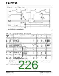
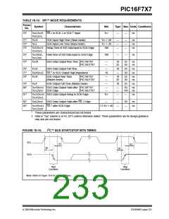
TABLE 18-8: CAPTURE/COMPARE/PWM REQUIREMENTS (ALL CCP MODULES)
Param
No.
Symbol
Characteristic
Min
Typ† Max Units
Conditions
50*
TCCL
CCP1, CCP2 and No prescaler
CCP3 Input Low
Time
0.5 TCY + 20
—
—
—
—
—
—
—
—
—
—
—
—
—
—
ns
ns
ns
ns
ns
ns
With prescaler PIC16F7X7
10
PIC16LF7X7
20
0.5 TCY + 20
10
51*
TCCH
CCP1, CCP2 and No prescaler
CCP3 Input High
With prescaler PIC16F7X7
PIC16LF7X7
Time
20
52*
53*
TCCP
TCCR
CCP1, CCP2 and CCP3 Input Period
3 TCY + 40
N
ns N = prescale
value (1, 4 or 16)
CCP1, CCP2 and CCP3 Output
Rise Time
PIC16F7X7
—
—
—
—
10
25
10
25
25
50
25
45
ns
ns
ns
ns
PIC16LF7X7
PIC16F7X7
PIC16LF7X7
54*
TCCF
CCP1, CCP2 and CCP3 Output
Fall Time
*
These parameters are characterized but not tested.
†
Data in “Typ” column is at 5V, 25°C unless otherwise stated. These parameters are for design guidance only and
are not tested.
2004 Microchip Technology Inc.
DS30498C-page 227

 MICROCHIP [ MICROCHIP ]