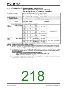
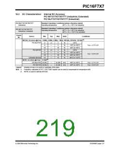
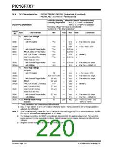
PIC16F7X7
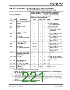
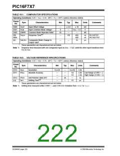
TABLE 18-1: COMPARATOR SPECIFICATIONS
Operating Conditions: 3.0V < VDD < 5.5V, -40°C < TA < +85°C (unless otherwise stated).
Param
No.
Sym
Characteristics
Input Offset Voltage
Min
Typ
Max
Units
Comments
D300
D301
D302
VIOFF
—
0
± 5.0
—
± 10
VDD – 1.5
—
mV
V
VICM
Input Common Mode Voltage*
Common Mode Rejection Ratio*
Response Time(1)*
CMRR
TRESP
55
—
—
dB
300
300A
150
400
600
ns
ns
PIC16F7X7
PIC16LF7X7
301
TMC2OV Comparator Mode Change to
Output Valid*
—
—
10
µs
*
These parameters are characterized but not tested.
Note 1: Response time measured with one comparator input at (VDD – 1.5)/2, while the other input transitions from
VSS to VDD.
TABLE 18-2: VOLTAGE REFERENCE SPECIFICATIONS
Operating Conditions: 3.0V < VDD < 5.5V, -40°C < TA < +85°C (unless otherwise stated).
Param
No.
Sym
Characteristics
Resolution
Min
Typ
Max
Units
Comments
D310
D311
VRES
VDD/24
—
VDD/32
LSb
VRAA
Absolute Accuracy
—
—
—
—
1/4
1/2
LSb
LSb
Low Range (CVRR = 1)
High Range (CVRR = 0)
D312
310
VRUR
TSET
Unit Resistor Value (R)*
Settling Time(1)*
—
—
2k
—
—
Ω
µs
10
*
These parameters are characterized but not tested.
Note 1: Settling time measured while CVRR = 1and CVR<3:0> transition from ‘0000’ to ‘1111’.
DS30498C-page 220
2004 Microchip Technology Inc.

 MICROCHIP [ MICROCHIP ]