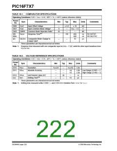
PIC16F7X7
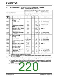
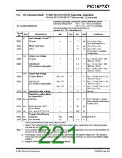
18.4 DC Characteristics: PIC16F737/747/767/777 (Industrial, Extended)
PIC16LF737/747/767/777 (Industrial) (Continued)
Standard Operating Conditions (unless otherwise stated)
Operating temperature
-40°C ≤ TA ≤ +85°C for industrial
-40°C ≤ TA ≤ +125°C for extended
DC CHARACTERISTICS
Param
Operating voltage VDD range as described in
Section 18.1 “DC Characteristics”.
Sym
Characteristic
Min
Typ†
Max Units
Conditions
No.
IIL
Input Leakage Current(2, 3)
D060
I/O ports
—
—
1
µA VSS ≤ VPIN ≤ VDD,
pin at high-impedance
D061
D063
MCLR, RA4/T0CKI
OSC1
—
—
—
—
5
5
µA VSS ≤ VPIN ≤ VDD
µA VSS ≤ VPIN ≤ VDD,
XT, HS and LP oscillator
configuration
VOL
Output Low Voltage
D080
D083
I/O ports
—
—
—
—
—
—
0.6
0.6
0.6
V
V
V
IOL = 8.5 mA, VDD = 4.5V,
-40°C to +125°C
OSC2/CLKO
(RC oscillator configuration)
IOL = 1.6 mA, VDD = 4.5V,
-40°C to +125°C
IOL = 1.2 mA, VDD = 4.5V,
-40°C to +125°C
VOH
Output High Voltage
D090
D092
I/O ports (Note 3)
VDD – 0.7
VDD – 0.7
VDD – 0.7
—
—
—
—
—
—
—
—
12
V
V
V
V
IOH = -3.0 mA, VDD = 4.5V,
-40°C to +125°C
IOH = -1.3 mA, VDD = 4.5V,
-40°C to +125°C
IOH = -1.0 mA, VDD = 4.5V,
-40°C to +125°C
OSC2/CLKO
(RC oscillator configuration)
D150* VOD Open-Drain High Voltage
RA4 pin
Capacitive Loading Specs
on Output Pins
D100 COSC2 OSC2 pin
—
—
15
pF In XT, HS and LP modes
when external clock is used
to drive OSC1
D101 CIO
D102 CB
All I/O pins and OSC2
(in RC mode)
SCL, SDA in I2C™ mode
Program Flash Memory
Endurance
—
—
—
—
50
pF
400
pF
D130 EP
100
2.0
1000
—
—
E/W 25°C at 5V
D131 VPR
VDD for Read
5.5
V
*
These parameters are characterized but not tested.
†
Data in “Typ” column is at 5V, 25°C unless otherwise stated. These parameters are for design guidance
only and are not tested.
Note 1: In RC oscillator configuration, the OSC1/CLKI pin is a Schmitt Trigger input. It is not recommended that the
PIC16F7X7 be driven with external clock in RC mode.
2: The leakage current on the MCLR pin is strongly dependent on the applied voltage level. The specified
levels represent normal operating conditions. Higher leakage current may be measured at different input
voltages.
3: Negative current is defined as current sourced by the pin.
2004 Microchip Technology Inc.
DS30498C-page 219

 MICROCHIP [ MICROCHIP ]