PIC16F7X7
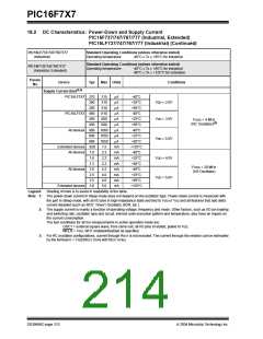
18.1 DC Characteristics: PIC16F737/747/767/777 (Industrial, Extended)
PIC16LF737/747/767/777 (Industrial)
Standard Operating Conditions (unless otherwise stated)
Operating temperature -40°C ≤ TA ≤ +85°C for industrial
PIC16LF737/747/767/777
(Industrial)
Standard Operating Conditions (unless otherwise stated)
PIC16F737/747/767/777
(Industrial, Extended)
Operating temperature
-40°C ≤ TA ≤ +85°C for industrial
-40°C ≤ TA ≤ +125°C for extended
Param
Sym
No.
Characteristic
Supply Voltage
Min
Typ† Max Units
Conditions
VDD
D001
PIC16LF7X7
2.5
2.2
2.0
—
—
—
5.5
5.5
5.5
V
V
V
A/D in use, -40°C to +85°C
A/D in use, 0°C to +85°C
A/D not used, -40°C to +85°C
D001
D001A
PIC16F7X7
4.0
VBOR*
—
—
5.5
5.5
V
V
All configurations
BOR enabled (Note 6)
D002*
VDR
RAM Data Retention
Voltage (Note 1)
—
1.5
—
V
D003
VPOR VDD Start Voltage to
ensure internal Power-on Reset
signal
—
VSS
—
V
See section on Power-on Reset for details
D004*
D005
SVDD VDD Rise Rate to ensure
0.05
—
—
V/ms See section on Power-on Reset for details
internal Power-on Reset signal
VBOR Brown-out Reset Voltage
PIC16LF7X7
BORV1:BORV0 = 11
BORV1:BORV0 = 10
BORV1:BORV0 = 01
BORV1:BORV0 = 00
1.96
2.06 2.16
2.78 2.92
4.33 4.55
4.64 4.87
V
V
V
V
85°C ≥ T ≥ 25°C
2.64
4.11
4.41
D005
PIC16F7X7 Industrial
BORV1:BORV0 = 1x
BORV1:BORV0 = 01
BORV1:BORV0 = 00
N.A.
—
—
—
N.A.
4.5
V
V
V
Not in operating voltage range of device
Not in operating voltage range of device
4.16
4.45
4.83
D005
PIC16F7X7 Extended
BORV1:BORV0 = 1x
BORV1:BORV0 = 01
BORV1:BORV0 = 00
N.A.
4.07
4.36
—
—
—
N.A.
4.59
4.92
V
V
V
Legend:
Shading of rows is to assist in readability of of the table.
These parameters are characterized but not tested.
*
†
Data in “Typ” column is at 5V, 25°C unless otherwise stated. These parameters are for design guidance only and are not
tested.
Note 1: This is the limit to which VDD can be lowered without losing RAM data.
2: The supply current is mainly a function of the operating voltage and frequency. Other factors, such as I/O pin loading and
switching rate, oscillator type, internal code execution pattern and temperature, also have an impact on the current
consumption.
The test conditions for all IDD measurements in active operation mode are:
OSC1 = external square wave, from-rail to-rail; all I/O pins tri-stated, pulled to VDD
MCLR = VDD; WDT enabled/disabled as specified.
3: The power-down current in Sleep mode does not depend on the oscillator type. Power-down current is measured with the
part in Sleep mode, with all I/O pins in high-impedance state and tied to VDD and VSS.
4: For RC oscillator configuration, current through REXT is not included. The current through the resistor can be estimated
by the formula Ir = VDD/2REXT (mA) with REXT in kΩ.
5: The ∆ current is the additional current consumed when this peripheral is enabled. This current should be added to the
base IDD or IPD measurement.
6: When BOR is enabled, the device will operate correctly until the VBOR voltage trip point is reached.
2004 Microchip Technology Inc.
DS30498C-page 209

 MICROCHIP [ MICROCHIP ]