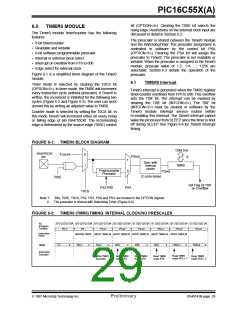
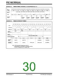
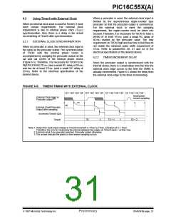
PIC16C55X(A)
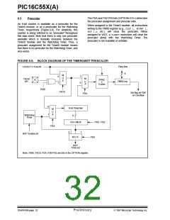
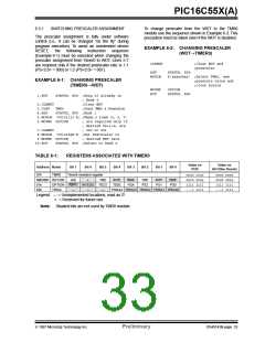
6.3.1
SWITCHING PRESCALER ASSIGNMENT
To change prescaler from the WDT to the TMR0
module use the sequence shown in Example 6-2. This
precaution must be taken even if the WDT is disabled.
The prescaler assignment is fully under software
control (i.e., it can be changed “on the fly” during
program execution). To avoid an unintended device
EXAMPLE 6-2: CHANGING PRESCALER
RESET,
the
following
instruction
sequence
(WDT→TIMER0)
(Example 6-1) must be executed when changing the
prescaler assignment from Timer0 to WDT. Lines 5-7
are required only if the desired postscaler rate is 1:1
(PS<2:0> = 000) or 1:2 (PS<2:0> = 001).
CLRWDT
;Clear WDT and
;prescaler
BSF
STATUS, RP0
MOVLW
b'xxxx0xxx' ;Select TMR0, new
;prescale value and
;clock source
OPTION
STATUS, RP0
EXAMPLE 6-1: CHANGING PRESCALER
(TIMER0→WDT)
MOVWF
BCF
1.BCF
STATUS, RP0 ;Skip if already in
; Bank 0
2.CLRWDT
3.CLRF
4.BSF
;Clear WDT
;Clear TMR0 & Prescaler
STATUS, RP0 ;Bank 1
TMR0
5.MOVLW '00101111’b; ;These 3 lines (5, 6, 7)
6.MOVWF OPTION
; are required only if
; desired PS<2:0> are
; 000 or 001
7.CLRWDT
8.MOVLW '00101xxx’b ;Set Postscaler to
9.MOVWF OPTION ; desired WDT rate
10.BCF STATUS, RP0 ;Return to Bank 0
TABLE 6-1:
REGISTERS ASSOCIATED WITH TIMER0
Value on
POR
Value on
All Other Resets
Address Name
Bit 7
Bit 6
Bit 5
Bit 4
Bit 3
Bit 2
Bit 1
Bit 0
01h
TMR0
Timer0 module’s register
GIE T0IE
OPTION RBPU INTEDG T0CS
TRISA
uuuu uuuu
0000 000x
1111 1111
---1 1111
xxxx xxxx
0000 000x
1111 1111
---1 1111
0Bh/8Bh INTCON
+
INTE
T0SE
RBIE
PSA
T0IF
PS2
INTF
PS1
RBIF
PS0
81h
85h
—
—
—
TRISA4 TRISA3 TRISA2 TRISA1 TRISA0
Legend: — = Unimplemented locations, read as ‘0’.
+ = Reserved for future use.
Note: Shaded bits are not used by TMR0 module.
1997 Microchip Technology Inc.
Preliminary
DS40143B-page 33

 MICROCHIP [ MICROCHIP ]