PIC16F872
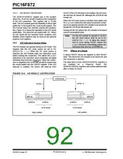
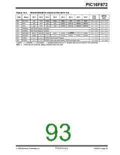
TABLE 10-2: REGISTERS/BITS ASSOCIATED WITH A/D
POR,
BOR
MCLR,
WDT
Addr
Name
Bit 7
Bit 6
Bit 5
Bit 4
Bit 3
Bit 2
Bit 1
Bit 0
0Bh
INTCON
PIR1
GIE
PEIE
ADIF
ADIE
T0IE
(1)
INTE
(1)
RBIE
SSPIF
SSPIE
T0IF
INTF
RBIF
0000 000x
r0rr 0000
r0rr 0000
xxxx xxxx
xxxx xxxx
0000 00-0
--0- 0000
--11 1111
--0x 0000
0000 000u
r0rr 0000
r0rr 0000
uuuu uuuu
uuuu uuuu
0000 00-0
--0- 0000
--11 1111
--0u 0000
0Ch
8Ch
1Eh
9Eh
1Fh
9Fh
85h
05h
(1)
CCP1IF
CCP1IE
TMR2IF
TMR1IF
PIE1
(1)
(1)
TMR2IE TMR1IE
(1)
ADRESH
ADRESL
ADCON0
ADCON1
TRISA
A/D Result Register High Byte
A/D Result Register Low Byte
ADCS1
ADFM
—
ADCS0
—
CHS2
CHS1
CHS0
GO/DONE
—
ADON
—
—
PCFG3
PCFG2
PCFG1
PCFG0
—
PORTA Data Direction Register
PORTA Data Latch when written: PORTA pins when read
PORTA
—
—
Legend: x= unknown, u= unchanged, -= unimplemented read as ’0’. Shaded cells are not used for A/D conversion.
Note 1: These bits are reserved; always maintain these bits clear.
1999 Microchip Technology Inc.
Preliminary
DS30221A-page 93

 MICROCHIP [ MICROCHIP ]