PIC16F872
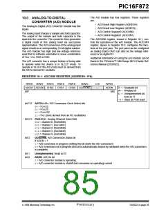
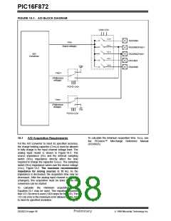
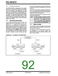
FIGURE 10-1: A/D BLOCK DIAGRAM
CHS<2:0>
100
RA5/AN4
VAIN
011
010
001
000
(Input voltage)
RA3/AN3/VREF+
RA2/AN2/VREF-
RA1/AN1
A/D
Converter
VDD
RA0/AN0
VREF+
(Reference
voltage)
PCFG<3:0>
VREF-
(Reference
voltage)
VSS
PCFG<3:0>
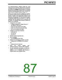
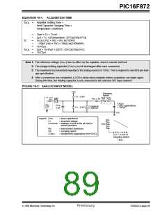
To calculate the minimum acquisition time, TACQ, see
the PICmicro™ Mid-Range Reference Manual
(DS33023).
10.1
A/D Acquisition Requirements
For the A/D converter to meet its specified accuracy,
the charge holding capacitor (CHOLD) must be allowed
to fully charge to the input channel voltage level. The
analog input model is shown in Figure 10-2. The
source impedance (RS) and the internal sampling
switch (RSS) impedance directly affect the time
required to charge the capacitor CHOLD. The sampling
switch (RSS) impedance varies over the device voltage
(VDD), Figure 10-2. The maximum recommended
impedance for analog sources is 10 kΩ. As the
impedance is decreased, the acquisition time may be
decreased. After the analog input channel is selected
(changed), this acquisition must be done before the
conversion can be started.
To calculate the minimum acquisition time,
Equation 10-1 may be used. This equation assumes
that 1/2 LSb error is used (1024 steps for the A/D). The
1/2 LSb error is the maximum error allowed for the A/D
to meet its specified resolution.
DS30221A-page 88
Preliminary
1999 Microchip Technology Inc.

 MICROCHIP [ MICROCHIP ]