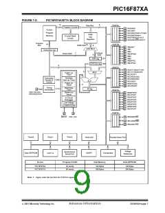
PIC16F87XA
TABLE 1-3:
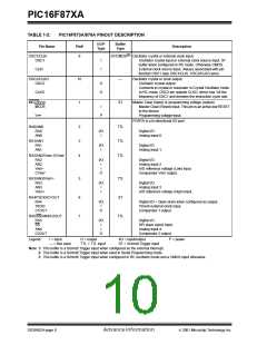
PIC16F874A/877A PINOUT DESCRIPTION (CONTINUED)
DIP
Pin#
PLCC
Pin#
QFP
Pin#
I/O/P
Type
Buffer
Type
Pin Name
Description
PORTB is a bi-directional I/O port. PORTB can be soft-
ware programmed for internal weak pull-up on all inputs.
(1)
RB0/INT
RB0
33
36
8
TTL/ST
I/O
I
Digital I/O.
External interrupt.
INT
I/O
I/O
RB1
RB2
34
35
36
37
38
39
9
TTL
TTL
TTL
Digital I/O.
Digital I/O.
10
11
RB3/PGM
RB3
I/O
I/O
Digital I/O.
PGM
Low voltage ICSP programming enable pin.
I/O
I/O
RB4
RB5
37
38
39
41
42
43
14
15
16
TTL
TTL
Digital I/O.
Digital I/O.
(2)
(2)
RB6/PGC
RB6
TTL/ST
I/O
I/O
Digital I/O.
PGC
In-Circuit Debugger and ICSP programming clock.
RB7/PGD
RB7
40
44
17
TTL/ST
I/O
I/O
Digital I/O.
PGD
In-Circuit Debugger and ICSP programming data.
PORTC is a bi-directional I/O port.
RC0/T1OSO/T1CKI
RC0
15
16
16
18
32
35
ST
ST
I/O
O
I
Digital I/O.
Timer1 oscillator output.
Timer1 external clock input.
T1OSO
T1CKI
RC1/T1OSI/CCP2
RC1
I/O
I
Digital I/O.
Timer1 oscillator input.
T1OSI
CCP2
I/O
Capture2 input, Compare2 output, PWM2 output.
RC2/CCP1
RC2
17
18
19
20
36
37
ST
ST
I/O
I/O
Digital I/O.
CCP1
Capture1 input/Compare1 output/PWM1 output.
RC3/SCK/SCL
RC3
I/O
I/O
I/O
Digital I/O.
SCK
SCL
Synchronous serial clock input/output for SPI mode.
Synchronous serial clock input/output for I C mode.
2
RC4/SDI/SDA
RC4
23
25
42
ST
I/O
I
I/O
Digital I/O.
SDI
SDA
SPI data in.
2
I C data I/O.
RC5/SDO
RC5
24
25
26
27
43
44
ST
ST
I/O
O
Digital I/O.
SPI data out.
SDO
RC6/TX/CK
RC6
TX
CK
I/O
O
I/O
Digital I/O.
USART asynchronous transmit.
USART 1 synchronous clock.
RC7/RX/DT
26
29
1
ST
RC7
RX
DT
I/O
I
I/O
Digital I/O.
USART asynchronous receive.
USART synchronous data.
Legend: I = input
O = output
— = Not used
I/O = input/output
TTL = TTL input
P = power
ST = Schmitt Trigger input
Note 1:This buffer is a Schmitt Trigger input when configured as an external interrupt.
2: This buffer is a Schmitt Trigger input when used in Serial Programming mode.
3: This buffer is a Schmitt Trigger input when configured as general purpose I/O and a TTL input when used in the Parallel
Slave Port mode (for interfacing to a microprocessor bus).
4: This buffer is a Schmitt Trigger input when configured in RC oscillator mode and a CMOS input otherwise.
2001 Microchip Technology Inc.
Advance Information
DS39582A-page 11

 MICROCHIP [ MICROCHIP ]