PIC16F87XA
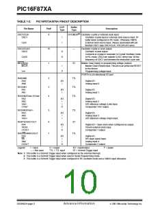
TABLE 1-2:
PIC16F873A/876A PINOUT DESCRIPTION
I/O/P
Type
Buffer
Type
Pin Name
Pin#
Description
(3)
OSC1/CLKI
OSC1
9
ST/CMOS
Oscillator crystal or external clock input.
I
I
Oscillator crystal input or external clock source input. ST
buffer when configured in RC mode. Otherwise CMOS.
External clock source input. Always associated with pin
function OSC1 (see OSC1/CLKI, OSC2/CLKO pins).
CLKI
OSC2/CLKO
OSC2
10
1
—
Oscillator crystal or clock output.
O
O
Oscillator crystal output.
Connects to crystal or resonator in Crystal Oscillator mode.
In RC mode, OSC2 pin outputs CLKO, which has 1/4 the
frequency of OSC1 and denotes the instruction cycle rate.
CLKO
MCLR/VPP
MCLR
ST
Master Clear (input) or programming voltage (output)
Master Clear (Reset) input. This pin is an active low RESET
to the device.
I
VPP
P
Programming voltage input.
PORTA is a bi-directional I/O port.
RA0/AN0
RA0
2
3
4
TTL
TTL
TTL
I/O
I
Digital I/O.
Analog input 0.
AN0
RA1/AN1
RA1
I/O
I
Digital I/O.
Analog input 1.
AN1
RA2/AN2/VREF-/CVREF
RA2
I/O
Digital I/O.
AN2
VREF-
CVREF
I
I
O
Analog input 2.
A/D reference voltage (Low) input.
Comparator VREF output.
RA3/AN3/VREF+
RA3
5
6
7
TTL
ST
I/O
I
I
Digital I/O.
Analog input 3.
A/D reference voltage (High) input .
AN3
VREF+
RA4/T0CKI/C1OUT
RA4
I/O
I
O
Digital I/O – Open drain when configured as output.
Timer0 external clock input.
Comparator 1 output.
T0CKI
C1OUT
RA5/SS/AN4/C2OUT
TTL
RA5
I/O
Digital I/O.
SS
AN4
I
I
SPI slave select input.
Analog input 4.
C2OUT
O
Comparator 2 output.
Legend:
I = input
— = Not used
O = output
TTL = TTL input
I/O = input/output
ST = Schmitt Trigger input
P = power
Note 1: This buffer is a Schmitt Trigger input when configured as the external interrupt.
2: This buffer is a Schmitt Trigger input when used in Serial Programming mode.
3: This buffer is a Schmitt Trigger input when configured in RC oscillator mode and a CMOS input otherwise.
DS39582A-page 8
AdvanceInformation
2001 Microchip Technology Inc.

 MICROCHIP [ MICROCHIP ]