PIC16F/LF1946/47
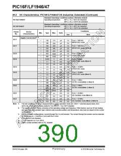
29.1 DC Characteristics: PIC16F/LF1946/47-I/E (Industrial, Extended)
Standard Operating Conditions (unless otherwise stated)
Operating temperature
-40°C TA +85°C for industrial
-40°C TA +125°C for extended
Standard Operating Conditions (unless otherwise stated)
PIC16F1946/47
Operating temperature
-40°C TA +85°C for industrial
-40°C TA +125°C for extended
Param.
No.
Sym.
Characteristic
Supply Voltage
Min.
Typ† Max.
Units
Conditions
D001
VDD
PIC16LF1946/47
1.8
2.3
—
—
3.6
3.6
V
V
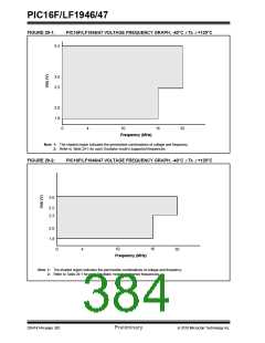
FOSC 16 MHz:
FOSC 32 MHz (NOTE 2)
D001
PIC16F1946/47
1.8
2.3
—
—
5.5
5.5
V
V
FOSC 16 MHz:
FOSC 32 MHz (NOTE 2)
D002*
VDR
RAM Data Retention Voltage(1)
PIC16LF1946/47
1.5
1.7
—
—
—
—
—
—
V
V
V
Device in Sleep mode
Device in Sleep mode
D002*
PIC16F1946/47
Power-on Reset Release Voltage
Power-on Reset Rearm Voltage
PIC16LF1946/47
VPOR*
1.6
VPORR*
—
—
0.8
1.7
—
—
V
V
Device in Sleep mode
Device in Sleep mode
PIC16F1946/47
D003
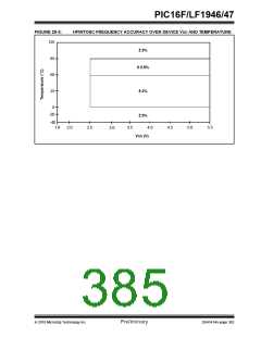
VADFVR
Fixed Voltage Reference Voltage
for ADC, Initial Accuracy
-6
-7
-7
-8
-7
-8
—
—
—
—
—
—
4
4
6
6
4
4
%
1.024V, VDD 1.8V, 85°C(3)
1.024V, VDD 1.8V, 125°C(3)
2.048V, VDD 2.5V, 85°C
2.048V, VDD 2.5V, 125°C
4.096V, VDD 4.75V, 85°C
4.096V, VDD 4.75V, 125°C
D003A
D003B
VCDAFVR
Fixed Voltage Reference Voltage
for Comparator and DAC, Initial
Accuracy
-7
-8
-8
-9
-8
-8
—
—
—
—
—
—
5
5
7
7
4
4
%
1.024V, VDD 1.8V, 85°C
1.024V, VDD 1.8V, 125°C
2.048V, VDD 2.5V, 85°C
2.048V, VDD 2.5V, 125°C
4.096V, VDD 4.75V, 85°C
4.096V, VDD 4.75V, 125°C
VLCDFVR
Fixed Voltage Reference Voltage
for LCD Bias, Initial Accuracy
-9
-9.5
—
—
9
9
%
3.072V, VDD 3.6V, 85°C
3.072V, VDD 3.6V, 125°C
D003C* TCVFVR
Temperature Coefficient, Fixed
Voltage Reference
—
-130
0.270
—
—
—
—
ppm/°C
%/V
D003D* VFVR/
VIN
Line Regulation, Fixed Voltage Ref-
erence
—
D004*
SVDD
VDD Rise Rate to ensure internal
0.05
V/ms
See Section 6.1 “Power-on Reset
(POR)” for details.
Power-on Reset signal
*
These parameters are characterized but not tested.
†
Data in “Typ” column is at 3.3V, 25°C unless otherwise stated. These parameters are for design guidance only and are not
tested.
Note 1: This is the limit to which VDD can be lowered in Sleep mode without losing RAM data.
2: PLL required for 32 MHz operation.
3: Selection not usable as ADC reference voltage.
DS41414A-page 384
Preliminary
2010 Microchip Technology Inc.

 MICROCHIP [ MICROCHIP ]