MCP41XXX/42XXX
Absolute Maximum Ratings †
VDD...................................................................................7.0V
All inputs and outputs w.r.t. VSS ............... -0.6V to VDD +1.0V
Storage temperature.....................................-60°C to +150°C
Ambient temp. with power applied................-60°C to +125°C
ESD protection on all pins..................................................≥ 2 kV
† Notice: Stresses above those listed under “maximum rat-
ings” may cause permanent damage to the device. This is a
stress rating only and functional operation of the device at
those or any other conditions above those indicated in the
operational listings of this specification is not implied. Expo-
sure to maximum rating conditions for extended periods may
affect device reliability.
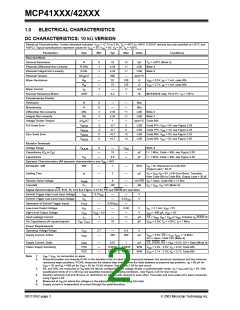
AC TIMING CHARACTERISTICS
Electrical Characteristics: Unless otherwise indicated, V = +2.7V to 5.5V, T = -40°C to +85°C.
DD
A
Parameter
Sym
Min.
Typ.
Max.
Units
Conditions
= 5V (Note 1)
Clock Frequency
Clock High Time
Clock Low Time
F
—
40
40
40
40
10
—
—
—
—
—
—
—
—
—
—
—
—
—
—
—
—
10
—
—
—
—
—
80
—
—
—
—
—
—
—
—
—
MHz
ns
ns
ns
ns
ns
ns
ns
ns
ns
ns
ns
ns
ns
ns
ns
V
DD
CLK
t
HI
t
LO
CS Fall to First Rising CLK Edge
Data Input Setup Time
Data Input Hold Time
SCK Fall to SO Valid Propagation Delay
SCK Rise to CS Rise Hold Time
SCK Rise to CS Fall Delay
CS Rise to CLK Rise Hold
CS High Time
t
CSSR
t
t
t
SU
HD
DO
C = 30 pF (Note 2)
L
t
30
10
100
40
150
150
40
100
150
CHS
t
t
t
CS0
CS1
CSH
Reset Pulse Width
t
Note 2
Note 2
Note 3
Note 3
Note 3
RS
RS Rising to CS Falling Delay Time
CS rising to RS or SHDN falling delay time
CS low time
t
RSCS
t
SE
t
CSL
Shutdown Pulse Width
t
SH
Note 1:
When using the device in the daisy-chain configuration, maximum clock frequency is determined by a combination of propagation delay
time (t ) and data input setup time (t ). Max. clock frequency is therefore ~ 5.8 MHz based on SCK rise and fall times of 5 ns, t
=
HI
DO
SU
40 ns, t = 80 ns and t = 40 ns.
DO
SU
2:
3:
Applies only to the MCP42XXX devices.
Applies only when using hardware pins to exit software shutdown mode, MCP42XXX only.
2003 Microchip Technology Inc.
DS11195C-page 5

 MICROCHIP [ MICROCHIP ]