MCP414X/416X/424X/426X
5.2
Wiper
5.3
WiperLock™ Technology
Each tap point (between the RS resistors) is a
connection point for an analog switch. The opposite
side of the analog switch is connected to a common
signal which is connected to the Terminal W (Wiper)
pin.
The MCP4XXX device’s WiperLock technology allows
application-specific calibration settings to be secured in
the EEPROM without requiring the use of an additional
write-protect pin. There are two WiperLock Technology
configuration bits (WL0 and WL1). These bits prevent
the Non-Volatile and Volatile addresses and bits for the
specified resistor network from being written.
A value in the volatile wiper register selects which
analog switch to close, connecting the W terminal to
the selected node of the resistor ladder.
The WiperLock technology prevents the serial
commands from doing the following:
The wiper can connect directly to Terminal B or to
Terminal A. A zero-scale connections, connects the
Terminal W (wiper) to Terminal B (wiper setting of
000h). A full-scale connections, connects the Terminal
W (wiper) to Terminal A (wiper setting of 100h or 80h).
In these configurations the only resistance between the
Terminal W and the other Terminal (A or B) is that of the
analog switches.
• Changing a volatile wiper value
• Writing to a non-volatile wiper memory location
• Changing the volatile TCON register value
For either Resistor Network 0 or Resistor Network 1
(Potx), the WLx bit controls the following:
• Non-Volatile Wiper Register
• Volatile Wiper Register
• Volatile TCON register bits RxHW, RxA, RxW, and
RxB
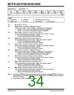
A wiper setting value greater than full scale (wiper
setting of 100h for 8-bit device or 80h for 7-bit devices)
will also be a Full Scale setting (Terminal W (wiper)
connected to Terminal A). Table 5-1 illustrates the full
wiper setting map.
High Voltage commands are required to enable and
disable WiperLock. Please refer to the Modify Write
Protect or WiperLock Technology (High Voltage)
command for operation.
Equation 5-2 illustrates the calculation used to deter-
mine the resistance between the wiper and terminal B.
5.3.1
POR/BOR OPERATION WHEN
WIPERLOCK TECHNOLOGY
ENABLED
EQUATION 5-2:
R
CALCULATION
WB
RAB
N
RWB = ------------- + RW
8-bit Device
The WiperLock Technology state is not affected by a
POR/BOR event. A POR/BOR event will load the
Volatile Wiper register value with the Non-Volatile
Wiper register value, refer to Section 4.1.
(256)
N = 0 to 256 (decimal)
RAB
N
7-bit Device
RWB = ------------- + RW
(128)
N = 0 to 128 (decimal)
TABLE 5-1:
VOLATILE WIPER VALUE VS.
WIPER POSITION MAP
Wiper Setting
7-bit Pot 8-bit Pot
Properties
3FFh
081h
3FFh
101h
Reserved (Full Scale (W = A)),
Increment and Decrement
commands ignored
080h
100h
Full Scale (W = A),
Increment commands ignored
07Fh
041h
0FFh
081
W = N
040h
080h
W = N (Mid-Scale)
W = N
03Fh
001h
07Fh
001
000h
000h
Zero Scale (W = B)
Decrement command ignored
DS22059B-page 36
© 2008 Microchip Technology Inc.

 MICROCHIP [ MICROCHIP ]