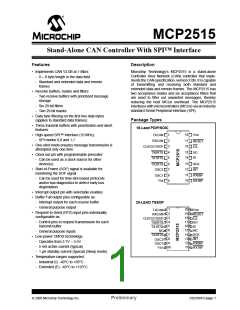
MCP2515
1.2
Control Logic
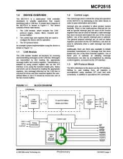
1.0
DEVICE OVERVIEW
The control logic block controls the setup and operation
of the MCP2515 by interfacing to the other blocks in
order to pass information and control.
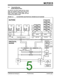
The MCP2515 is a stand-alone CAN controller
developed to simplify applications that require
interfacing with a CAN bus. A simple block diagram of
the MCP2515 is shown in Figure 1-1. The device
consists of three main blocks:
Interrupt pins are provided to allow greater system
flexibility. There is one multi-purpose interrupt pin (as
well as specific interrupt pins) for each of the receive
registers that can be used to indicate a valid message
has been received and loaded into one of the receive
buffers. Use of the specific interrupt pins is optional.
The general purpose interrupt pin, as well as status
registers (accessed via the SPI interface), can also be
used to determine when a valid message has been
received.
1. The CAN module, which includes the CAN
protocol engine, masks, filters, transmit and
receive buffers.
2. The control logic and registers that are used to
configure the device and its operation.
3. The SPI protocol block.
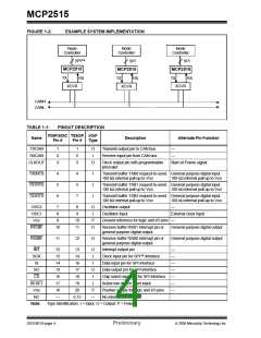
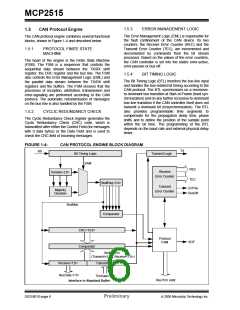
An example system implementation using the device is
shown in Figure 1-2.
Additionally, there are three pins available to initiate
immediate transmission of a message that has been
loaded into one of the three transmit registers. Use of
these pins is optional, as initiating message
transmissions can also be accomplished by utilizing
control registers, accessed via the SPI interface.
1.1
CAN Module
The CAN module handles all functions for receiving
and transmitting messages on the CAN bus. Messages
are transmitted by first loading the appropriate
message buffer and control registers. Transmission is
initiated by using control register bits via the SPI
interface or by using the transmit enable pins. Status
and errors can be checked by reading the appropriate
registers. Any message detected on the CAN bus is
checked for errors and then matched against the user-
defined filters to see if it should be moved into one of
the two receive buffers.
1.3
SPI Protocol Block
The MCU interfaces to the device via the SPI interface.
Writing to, and reading from, all registers is
accomplished using standard SPI read and write
commands, in addition to specialized SPI commands.
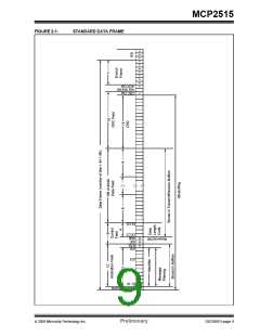
FIGURE 1-1:
BLOCK DIAGRAM
CAN Module
RXCAN
TXCAN
CAN
Protocol
Engine
CS
SCK
SI
SPI™
Interface
Logic
TX and RX Buffers
Masks and Filters
SPI
Bus
SO
Control Logic
OSC1
OSC2
Timing
Generation
INT
CLKOUT
RX0BF
RX1BF
TX0RTS
TX1RTS
TX2RTS
Control
and
Interrupt
Registers
RESET
© 2005 Microchip Technology Inc.
Preliminary
DS21801D-page 3

 MICROCHIP [ MICROCHIP ]