MCP1825/MCP1825S
AC/DC CHARACTERISTICS (CONTINUED)
Electrical Specifications: Unless otherwise noted, VIN = VOUT(MAX) + VDROPOUT(MAX), Note 1, VR = 1.8V for Adjustable Output,
I
OUT = 1 mA, CIN = COUT = 4.7 µF (X7R Ceramic), TA = +25°C.
Boldface type applies for junction temperatures, TJ (Note 7) of -40°C to +125°C
Parameters
Sym
Min
Typ
Max
350
Units
Conditions
Dropout Characteristics
Dropout Voltage
VDROPOUT
—
210
mV
Note 5, IOUT = 500 mA,
V
IN(MIN) = 2.1V
Power Good Characteristics
PWRGD Input Voltage Operat-
ing Range
VPWRGD_VIN
1.0
—
—
6.0
V
TA = +25°C
1.2
6.0
TA = -40°C to +125°C
For VIN < 2.1V, ISINK = 100 µA
PWRGD Threshold Voltage
VPWRGD_TH
%VOUT Falling Edge
VOUT < 2.5V Fixed,
OUT = Adj.
(Referenced to VOUT
)
89
92
95
V
90
1.0
—
92
2.0
0.2
94
3.0
0.4
VOUT >= 2.5V Fixed
PWRGD Threshold Hysteresis
PWRGD Output Voltage Low
VPWRGD_HYS
VPWRGD_L
%VOUT
V
IPWRGD SINK = 1.2 mA,
ADJ = 0V
PWRGD Leakage
PWRGD
_
—
—
1
—
—
nA
µs
VPWRGD = VIN = 6.0V
Rising Edge
LK
PWRGD Time Delay
TPG
110
RPULLUP = 10 kΩ
Detect Threshold to PWRGD
Active Time Delay
TVDET-PWRGD
—
200
—
µs
VOUT = VPWRGD_TH + 20 mV
to VPWRGD_TH - 20 mV
Shutdown Input
Logic High Input
VSHDN-HIGH
VSHDN-LOW
SHDNILK
45
—
—
—
—
15
%VIN
%VIN
µA
VIN = 2.1V to 6.0V
VIN = 2.1V to 6.0V
Logic Low Input
SHDN Input Leakage Current
-0.1
±0.001
+0.1
VIN = 6V, SHDN =VIN
SHDN = GND
,
AC Performance
Output Delay From SHDN
TOR
eN
—
—
100
2.0
—
—
µs
SHDN = GND to VIN
,
V
OUT = GND to 95% VR
Output Noise
µV/√Hz IOUT = 200 mA, f = 1 kHz,
OUT = 10 µF (X7R Ceramic),
OUT = 2.5V
C
V
Note 1: The minimum VIN must meet two conditions: VIN ≥ 2.1V and VIN ≥ VOUT(MAX) + VDROPOUT(MAX).
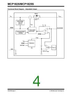
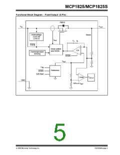
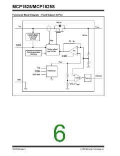
2: VR is the nominal regulator output voltage for the fixed cases. VR = 1.2V, 1.8V, etc. VR is the desired set point output
voltage for the adjustable cases. VR = VADJ * ((R1/R2)+1). Figure 4-1.
3: TCVOUT = (VOUT-HIGH – VOUT-LOW) *106 / (VR * ΔTemperature). VOUT-HIGH is the highest voltage measured over the
temperature range. VOUT-LOW is the lowest voltage measured over the temperature range.
4: Load regulation is measured at a constant junction temperature using low duty-cycle pulse testing. Load regulation is
tested over a load range from 1 mA to the maximum specified output current.
5: Dropout voltage is defined as the input-to-output voltage differential at which the output voltage drops 2% below its
nominal value that was measured with an input voltage of VIN = VOUT(MAX) + VDROPOUT(MAX)
.
6: The maximum allowable power dissipation is a function of ambient temperature, the maximum allowable junction
temperature and the thermal resistance from junction to air. (i.e., TA, TJ, θJA). Exceeding the maximum allowable power
dissipation will cause the device operating junction temperature to exceed the maximum +150°C rating. Sustained
junction temperatures above 150°C can impact device reliability.
7: The junction temperature is approximated by soaking the device under test at an ambient temperature equal to the
desired junction temperature. The test time is small enough such that the rise in the junction temperature over the
ambient temperature is not significant.
DS22056B-page 8
© 2008 Microchip Technology Inc.

 MICROCHIP [ MICROCHIP ]